
IATF 16949 Certified Manufacturer
Top 5 Critical Specs for EV Power Module Lead Frames
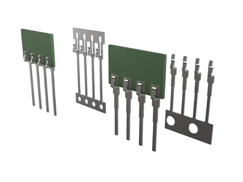
Table of Contents
A power module program recently scrapped 38,000 stamped lead frames because die pad coplanarity drifted to 0.06 mm after 400,000 die strokes. The silver sinter layer under the SiC die developed voids, thermal resistance climbed past the datasheet limit, and field returns started at 18 months. The sorting, rework and warranty reserve cost more than the entire tooling program.
Key Takeaways
- Die pad coplanarity prevents micro-voids and isolated thermal resistance in SiC chips.
- Strict die clearance and deburring eliminate micro-burrs that trigger catastrophic dielectric breakdown.
- Correct grain orientation and bend radii prevent propagating fatigue failures during thermal cycling.
EV power module lead frames look like simple stamped strips. They are not. A lead frame is the electrical interconnect, the thermal path, the handling backbone and the mold-sealing surface of the power module, all in one part. At 800V system voltage and hundreds of amperes, a 0.01 mm defect can end a module in the field.
This guide covers lead frame materials, tolerance capability and manufacturing for EV power modules, with production numbers you can take to a quote review. It is written for engineers and buyers evaluating EV power module lead frame stamping services.
The Snapshot
- C1100 ETP copper delivers 101% IACS; C194 and C7025 copper alloys add strength for thin lead frame strip.
- Alloy 42 (NiFe) matches the thermal expansion of ceramic and silicon to survive power cycling.
- Progressive die stamping holds ±0.005 mm on critical features; chemical etching holds ±0.025 mm typical.
- Die pad coplanarity below 0.05 mm and burr height below 15 μm (typical) protect die attach and 800V isolation.
- Selective plating applies silver or tin at 1 to 8 μm typical and gold at 0.1 to 1.5 μm typical only where needed.
What Is an EV Power Module Lead Frame?
A lead frame is a stamped metal strip that carries the power semiconductor dies of an EV power module. The dies attach to the die pads, bond wires connect them to the lead fingers, and the whole assembly is encapsulated in molding compound. The exposed lead ends become the module terminals.
In an EV, the power module sits inside the traction inverter, the on-board charger and the DC-DC converter. It switches hundreds of amperes at up to 800V system voltage. The 800V and silicon carbide shift changed the part completely: SiC dies switch faster, run hotter, and tolerate almost no voiding in their attach layer.
The lead frame performs four jobs at once:
- Electrical interconnect: it carries current from the DC bus to the chips and out to the load terminals.
- Thermal path: it conducts heat from the dies toward the baseplate and the cooling system.
- Mechanical backbone: it holds the chips and bond wires during assembly, handling and encapsulation.
- Sealing surface: it must seal against the molding compound so resin flash never reaches the bond zones.
Most lead frames run from copper alloy strip 0.1 to 0.3 mm thick (typical). Stamping lines produce them at up to 800 SPM on presses from 25 to 300 ton. The part is small, thin and cheap. The failure it can cause is not.
Why Lead Frames Fail in EV Power Modules
Every lead frame failure mode traces back to a dimension, a surface or an edge. Understanding the failure chain explains why the tolerances in the next sections are so tight. These are the four failure families that dominate field returns:
| Failure mode | Field symptom | Root cause in the lead frame | Verification method |
|---|---|---|---|
| Die attach voiding | Thermal runaway, derating in hot climates | Die pad coplanarity drift above 0.05 mm | Coplanarity gauge, X-ray of the sinter layer |
| Dielectric breakdown | Sudden inverter failure at high voltage | Burr over 15 μm on the stamped edge | Burr gauge, 10x to 20x optical inspection |
| Solder and sinter fatigue | Open circuit after thermal cycling | CTE mismatch between frame and ceramic | Power cycling test, cross-section |
| Bond lift-off | Intermittent signal, open circuit | Coining depth drift, surface roughness change | Wire pull test, coining depth probe |
| Resin flash and delamination | Package cracking after molding | Edge perpendicularity loss, worn die | Cross-section, thermal shock test |
Note the pattern. Each failure starts as a tolerance drift inside the stamping die, then becomes a field failure 18 to 36 months later. That is why lead frame quality is measured in capability data, not in certificates.
Lead Frame Materials for EV Power Modules
Material selection starts with two numbers: how much current the lead must carry, and how much thermal expansion mismatch the package can survive. The standard EV lead frame alloys:
| Alloy | Conductivity | CTE (typical) | Strength | Typical role |
|---|---|---|---|---|
| C1100 ETP copper | 101% IACS | ~17 ppm/°C | Soft, formable | High-current power leads, terminal tabs |
| C194 copper-iron | 60 to 65% IACS (typical) | ~17 ppm/°C | Medium-high | Workhorse lead frame strip for power modules |
| C7025 copper-nickel-silicon | 35 to 40% IACS (typical) | ~17.6 ppm/°C | High | Thin-pitch, high-strength SiC frames |
| C5210 phosphor bronze | 15% IACS | ~18 ppm/°C | High, springy | Clip leads, spring contacts |
| Alloy 42 (NiFe) | ~3.5% IACS (typical) | 4.5 to 5.2 ppm/°C | Medium | CTE-matched frames for ceramic packages |
Conductivity drives the current rating; CTE drives the survival of the solder and sinter joints. Copper conducts heat and current superbly, but it expands at roughly 17 ppm/°C (typical). Silicon carbide expands near 3 ppm/°C (typical), and aluminum nitride ceramic near 4.5 ppm/°C (typical). The gap between those numbers is the stress budget the package must absorb.
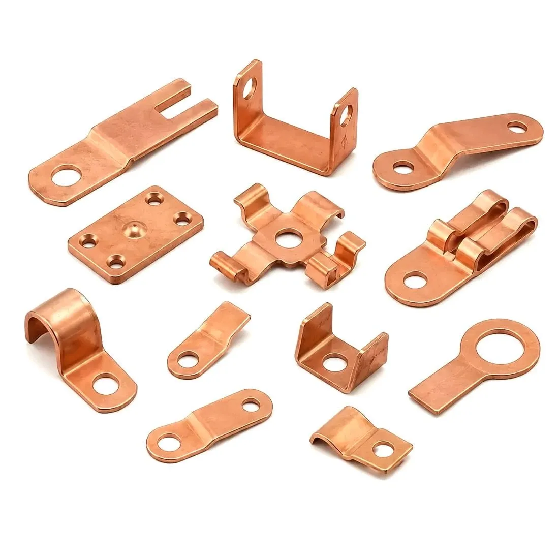
Material Selection Trade-offs: Conductivity vs CTE
No single alloy wins on every requirement. The trade-off ladder looks like this:
| Requirement | C1100 ETP | C194 | C7025 | Alloy 42 |
|---|---|---|---|---|
| Electrical conductivity | Excellent, 101% IACS | Good (typical) | Moderate (typical) | Low (typical) |
| CTE match to ceramic | Poor | Poor | Poor | Excellent |
| Strength at thin gauge | Low | Medium | High | Medium |
| Thermal cycling life | Low to medium | Medium | Medium | High |
| Relative material cost | Low | Medium | High | Medium |
| Typical module application | IGBT emitter leads | Main lead frame strip | Thin-pitch SiC frames | Sealed, CTE-critical packages |
Two practical rules follow. First, use the most conductive alloy that still holds the required strength, because current rating is a safety function. Second, when the package cannot absorb the CTE stress, switch the frame to Alloy 42, or redesign the lead geometry so copper leads flex instead of tearing the joint. A compliant lead design costs nothing in tooling and buys years of power cycling life.
The compromise most programs choose is C194: about 60 to 65% IACS (typical), enough strength for thin gauge, and a familiar stamping and plating behavior. C7025 appears when the lead pitch gets tight and the frame must stay rigid. Alloy 42 appears when the substrate is ceramic and the module cannot live with copper expansion. Both decisions belong in the DFM review, before tooling is cut.
Stamping vs Etching for Lead Frames
Lead frames can be made by progressive die stamping or by chemical etching. The two processes overlap on thin strip, but they do not overlap on tolerance, edge quality or cost curve. The comparison table:
| Factor | Progressive die stamping | Chemical etching |
|---|---|---|
| Critical dimension tolerance | ±0.005 to 0.01 mm (typical) | ±0.025 mm (typical) |
| Edge profile | Shear and burnish zones, controlled burr | Smooth, slightly tapered, burr-free |
| Burr control | Below 15 μm typical with tight die clearance | No mechanical burr |
| Production speed | Up to 800 SPM | Batch process, hours per panel |
| Tooling cost | USD 20,000 to 200,000+ (typical) | Low, film masks only |
| Tooling lead time | 4 to 6 weeks (typical) | Days to 2 weeks |
| Volume crossover | Wins above roughly 100,000 parts per year (typical) | Wins for prototyping and low volume |
| Material range | All lead frame alloys | All lead frame alloys |
Stamping wins wherever the volume is real, because unit cost collapses above the crossover and the tolerance is tighter. Etching wins for prototypes, pre-production and the first article. Some programs etch early and stamp in production, which is a clean way to de-risk a new lead frame design before the die is cut.
Burr deserves a special line. Etching leaves no mechanical burr, which is attractive for 800V isolation. Stamping can hold burr below 15 μm (typical) with correct die clearance, guidance and regrind intervals, and it does so at a fraction of the unit cost. The die design decides the burr, not the process name.
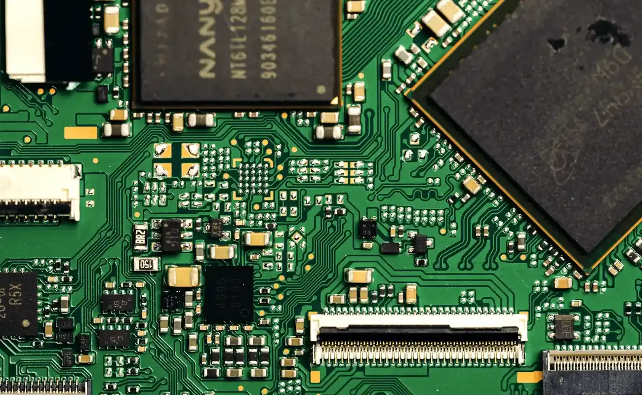
Critical Tolerances: Coplanarity, Burr and Flatness
Five numbers decide whether a lead frame program launches clean. They are the specification spine of the part:
| Characteristic | Typical requirement | What it protects |
|---|---|---|
| Die pad coplanarity | Below 0.05 mm | Void-free die attach and sinter layer |
| Burr height | Below 15 μm, or below 10% of material thickness | 800V dielectric isolation and mold sealing |
| Critical dimension tolerance | ±0.005 mm with Cpk ≥ 1.67 | Wire bond pitch, lead position, assembly |
| Frame thickness | 0.1 to 0.3 mm (typical) | Current capacity, stiffness, die attach surface |
| Measurement system | GR&R below 10% of the tolerance band | Capability numbers mean something |
Coplanarity is the first check on any new die. If the die pad rocks even slightly, the sinter or solder layer thickness varies, voids form, and the die overheats under load. Hold coplanarity below 0.05 mm and the attach process has a flat stage to work on. Modern silver sintering presses the die at high pressure, so a non-flat pad cracks the die before it ever sees current.
Burr is the second check. At 800V system voltage, a burr on a lead edge concentrates the electric field and can ionize the mold compound, which then arcs and tracks across the package. The practical rule is burr below 15 μm or below 10% of the material thickness (typical), measured at the press with a burr gauge, not in the lab after the fact.
The other three numbers are process hygiene: a real tolerance budget at ±0.005 mm on the critical features, a thickness that fits the current and stiffness targets, and a measurement system you can trust. GR&R below 10% of the tolerance band is the gate that makes Cpk data honest.
Plating Systems for Lead Frames
Plating is specified by function, and the function varies across one lead frame. The die attach zone needs a surface that sinters or solders reliably. The bond finger needs a surface that wire bonds without lift-off. The external leads need solderability after storage. Selective plating puts each metal only where it works:
| Plating | Thickness (typical) | Function | Typical zone |
|---|---|---|---|
| Silver (Ag), selective | 1 to 8 μm | Low contact resistance, sinter and solder surface | Die pads, bond fingers, high-current leads |
| Tin (Sn), selective or full | 1 to 8 μm | Solderability, corrosion barrier | External leads, solder joints |
| Gold (Au) | 0.1 to 1.5 μm | Oxidation-free wire bond surface | Bond fingers, signal contacts |
| Nickel (Ni) barrier | 1 to 10 μm | Diffusion barrier under silver and gold | Underlayers on copper strip |
Selective plating is where the cost is controlled. Masking limits silver and gold to the functional zones, cutting precious metal consumption by up to 90% compared to full plating. The mask registration against the stamped features is a tolerance in its own right, typically verified with optical measurement before plating.
Burr direction matters again at the plating line. A burr facing into the plated zone can shadow the deposit and create a pinhole. The die layout should place the burr on the side away from the plating surface, and the plating supplier should verify thickness by X-ray fluorescence on every lot.
The Lead Frame Stamping Process
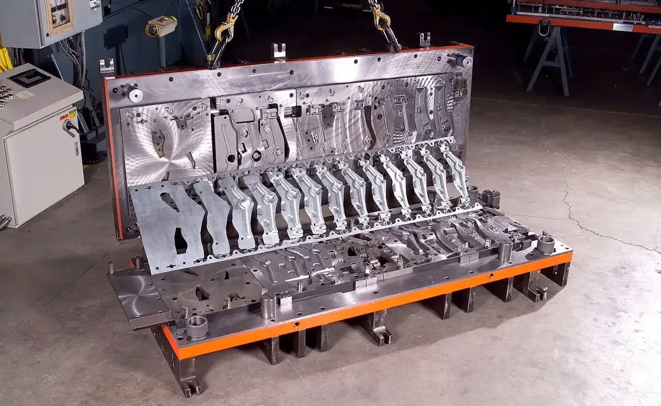
Progressive die stamping makes lead frames the same way it makes terminals, but with stricter dies and cleaner edges. Coil feeds a multi-station die, and every press stroke completes one part. The station sequence controls the features that fail in the field:
| Stage | Operation | What it controls |
|---|---|---|
| 1 | Blanking and piercing | Outer profile, holes, burr direction and size |
| 2 | Coining | Die pad flatness, local thickness, coplanarity |
| 3 | Forming and bending | Lead bends, stand-off height, springback compensation |
| 4 | Plating window and marking | Selective plating zone, lot trace codes |
| 5 | Cut-off and trim | Part separation, edge perpendicularity |
Presses from 25 to 300 ton cover the range, and high-speed lines run up to 800 SPM. Speed is not the risk; die rigidity is. A flexible die or a loose guide set shows up as coplanarity drift and burr growth long before it shows up as a broken punch. That is why die guidance, clearance control and regrind intervals are the real quality system.
Coining is the stage most lead frame buyers underweight. The die pad and the bond fingers are coined to a controlled thickness and flatness, because the die attach and wire bond processes are sensitive to both. Coining depth is checked with a probe or a CMM, and capability data at Cpk ≥ 1.67 is the acceptance gate. Springback on thin copper is small but never zero, so overbend compensation is built into the die and verified on the first article.
Quality Verification and Capability Data
Lead frame quality is verified with instruments, not with certificates. The verification stack for an EV power module lead frame program:
- Capability studies: 100-plus parts measured per critical dimension, with Cpk ≥ 1.67 required before production release.
- CMM measurement: coplanarity, lead position and pitch verified on a coordinate measuring machine at defined intervals.
- Burr gauging: burr height checked at the press with a burr gauge and 10x to 20x optical inspection.
- GR&R: gauge repeatability and reproducibility below 10% of the tolerance band, or the Cpk numbers are noise.
- Traceability: coil lot, press, die and shift recorded per batch, traceable from coil to shipment.
- PPAP documentation: control plans, FMEA and measurement system analysis delivered with the first article.
Ask any supplier for the GR&R study and the capability chart, not just the tolerance claim. The difference between a lead frame that launches clean and one that fails at 18 months is usually visible in that chart. In-line metrology catches die wear before the drift compounds into a sorting event.
Design for Manufacturing Rules
Small drawing decisions decide whether a lead frame runs at 800 SPM or fights the die. The rules that matter for EV lead frames:
| Design rule | Typical value | Why it matters |
|---|---|---|
| Minimum feature size | 0.3 to 0.5 mm (stamped) | Die construction and punch strength limits |
| Minimum bend radius | 1x stock thickness (copper alloys) | Below this, outer fibers crack |
| Tolerance callouts | Only critical dims at ±0.005 mm | Every tight tolerance is a die station and an inspection point |
| Burr direction | Away from die attach and plating surfaces | Prevents voiding, pinholes and 800V field concentration |
| Grain direction | Bends across the coil grain where possible | Parallel bends crack in hard alloys |
| Tie bars and rails | Keep frames attached for plating and handling | Reduces distortion, enables reel-to-reel processing |
The most expensive sentence on a lead frame drawing is a tight tolerance on a non-critical dimension. Spend the ±0.005 mm budget where the function lives: the die pad, the bond fingers and the lead pitch.
Cost Drivers for Lead Frame Programs
Lead frame cost breaks into the same buckets as any stamped electrical part, but the ratios shift:
| Cost driver | Share (typical) | Lever you control |
|---|---|---|
| Material | 40 to 60% of part cost | Strip layout, coil width, alloy grade |
| Tooling | USD 20,000 to 200,000+ amortized over volume | Committed volume, die feature scope |
| Plating | 10 to 25% of part cost | Selective zones, mask design |
| Process and inspection | In-die operations remove secondary vendors | Die scope, in-line metrology |
Material dominates because a lead frame is pure metal with high scrap sensitivity. A strip layout that nests parts tighter can cut material cost by 10 to 20% (typical) without touching the die. Plating is the second lever: selective silver and gold zones cut precious metal consumption by up to 90% versus full plating.
The crossover rule from the process section decides the tooling decision. Below roughly 100,000 parts per year (typical), etching or hybrid routes compete. Above it, progressive die stamping wins on unit cost by a wide margin.
How to Select a Lead Frame Stamping Supplier
Run this checklist before you send a lead frame drawing to any stamping manufacturer:
- Die ownership: an in-house toolroom that can iterate coplanarity and burr issues in days, not months. Tooling runs 4 to 6 weeks typical.
- Capability data: Cpk ≥ 1.67 studies and GR&R below 10% delivered before production, not on request.
- Material control: same-lot coils, incoming chemistry verification and batch trace codes for C194, C7025 and Alloy 42.
- Plating integration: selective plating with mask registration control and X-ray thickness verification.
- Measurement: CMM, coplanarity and burr gauging in-house, with SPC charts on the critical dimensions.
- Capacity fit: 25 to 300 ton presses and up to 800 SPM lines that match your volume curve.
A supplier that hands you the GR&R and Cpk data before you ask is running a quality system. One that promises it later is running a gamble with your module launch.
The Bottom Line
EV power module lead frames are small, thin and cheap. Their failure cost is not. The materials are copper alloys and NiFe, selected on the conductivity and CTE trade-off. The tolerances that matter are coplanarity below 0.05 mm, burr below 15 μm, and critical dimensions at ±0.005 mm with Cpk ≥ 1.67. Stamping wins above the volume crossover; etching covers prototyping and first articles. Hold your supplier to capability data, selective plating discipline and die ownership, and the module has a backbone it can survive on.
Work with a stamping partner that treats these numbers as contract items, not suggestions. Our lead frame stamping services cover progressive die capacity, in-house tooling and selective plating. The materials page details C1100, C194 and Alloy 42, and the blog carries more EV component engineering guides.
Send the drawing and this checklist together when you request a quote. The DFM review comes back with the numbers attached, including the items that need a design change. That is the difference between a lead frame that ships and one that survives.
NEXT STEP
Ready to Manufacture Your Part?
Send us your drawing or sample — our engineers return DFM feedback within 24 hours with pricing and lead time from our IATF 16949 factory.
Written by
Ray Chan
Manufacturing engineer at KRAVZIK (Dongguan Guohong Precision). Writes shop-floor guides on progressive-die stamping, injection molding and precision component sourcing for global OEM buyers.