
IATF 16949 Certified Manufacturer
The Engineer's Guide to EMI/RFI Shield DFM for Progressive Stamping
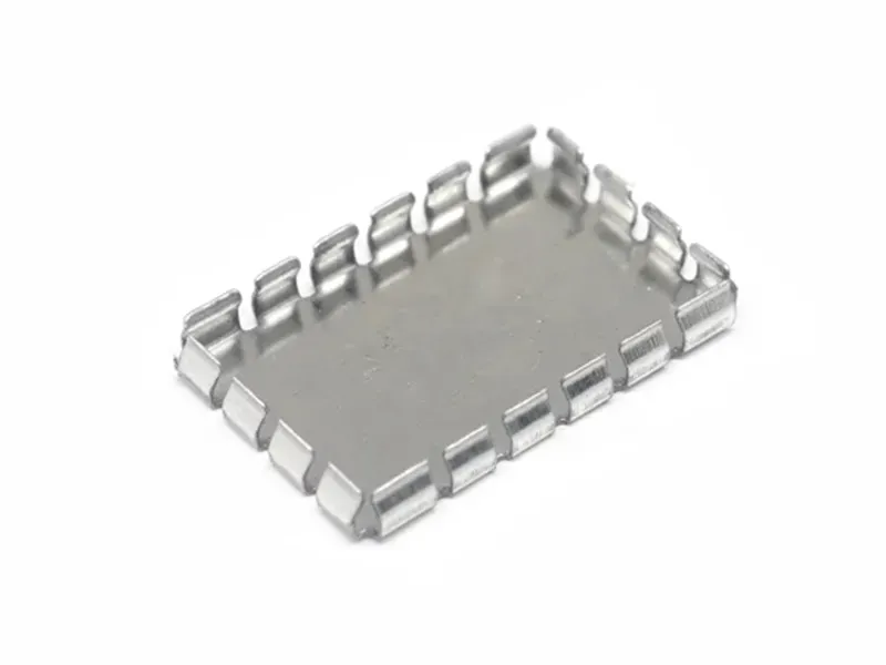
Table of Contents
An IoT gateway passed pre-compliance with 52 dB of measured shielding effectiveness. Three weeks later, the same product failed final radiated emission testing at 2.4 GHz. The only change was a die revision that enlarged the shield vent holes from 1.0 mm to 1.6 mm. Each hole now admitted 2.6 times more open area. The certification retest cost USD 18,000 (typical for a small product), and the launch slipped four weeks.
Key Takeaways
- Orient all flat blank bend lines perpendicular to the material grain to prevent micro-cracking.
- Design bend reliefs and maintain proper radii to prevent flange tearing and tooling breakage.
- Add stiffening ribs to flat surfaces to defeat thermal warping and guarantee SMT coplanarity.
The shield looked identical. It measured identically on a caliper. Its perforation grid just stopped behaving like a solid plane at 2.4 GHz. That is the gap between a stamped EMI shield and a DFM-correct one. The difference hides in holes, bends, contacts and tolerances that a drawing review will not catch.
This guide is the design for manufacturability (DFM) playbook for stamped EMI shields. It is written for hardware engineers, PCB designers and procurement teams. It covers materials, skin depth, aperture rules, grounding, tolerances, plating, tooling and cost. Every production number is labeled typical.
The Snapshot
- Stamped shields deliver 40-80 dB of shielding effectiveness in the 30-100 MHz band from 0.08-0.5 mm stock (typical)
- Skin depth at 100 MHz is about 6.6 µm in copper and 65 µm in magnetic steel (typical). Above 300 MHz, thickness is a stiffness decision, not a shielding one
- Keep every aperture below one twentieth of the wavelength at your highest frequency, about 6 mm at 2.4 GHz (typical guidance)
- Progressive dies hold critical dimensions to ±0.01-0.03 mm (typical) at up to 800 SPM on 25-300 ton presses
- SECC, SUS301 and AL5052 cover most shield programs; tin or nickel plating handles solderability and salt spray per ASTM B117 for 48-72 hours (typical)
Why EMI Shields Fail: The Test That Exposes Bad DFM
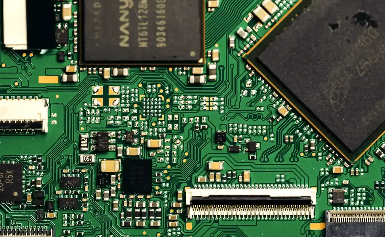
Radiated emission limits are the real customer for every shield. Commercial electronics typically must hold emissions below FCC Part 15 or CISPR limits. Receivers must also survive nearby transmitters. A shield that passes in the lab and fails in the module is almost always a DFM problem. Apertures, grounding or material changed during tooling.
Shielding effectiveness is measured in decibels. Every 20 dB is a tenfold reduction in field strength. A 40 dB shield stops 99 percent of the field. A 60 dB shield stops 99.9 percent. Stamped enclosures with good grounding typically land between 40 and 80 dB in the 30-100 MHz range. That band covers most immunity and emission work on real products.
The math behind the test is worth internalizing. A 3 dB shift doubles the field strength. A 6 dB shift quadruples it. Small mechanical changes, like a slightly larger hole grid, move the number far more than most teams expect.
| Shielding effectiveness | Field reduction | Typical stamped shield result |
|---|---|---|
| 20 dB | 90% | poor grounding, large apertures |
| 40 dB | 99% | solid panel with modest apertures |
| 60 dB | 99.9% | small holes, frequent ground contacts |
| 80 dB | 99.99% | solid walls, sealed seams, best practice |
Three factors set the number: reflection at the surface, absorption inside the material, and leakage through apertures and seams. DFM controls the third one. It is also the factor that drifts in production.
How a Stamped EMI Shield Works
A metal shield attenuates a field by reflection and by absorption. Reflection dominates in high-conductivity, non-magnetic metals like copper and aluminum. Absorption dominates in magnetic steel, which converts field energy into heat. Both mechanisms follow skin depth, the depth at which the field falls to about 37 percent of its surface value.
The skin depth formula is δ = 1 / √(π f μ σ). Here f is frequency, μ is permeability and σ is conductivity. Three practical lessons follow. First, skin depth shrinks as frequency rises, so thin material works at high frequency. Second, steel’s high permeability shrinks skin depth despite lower conductivity, which is why steel absorbs well. Third, material thicker than three skin depths behaves like a solid wall (typical rule of thumb).
Total shielding effectiveness is the sum of reflection loss, absorption loss and a re-reflection correction. Reflection depends on surface conductivity. Absorption depends on thickness and permeability. For a stamped shield in the 30-100 MHz band, both mechanisms work because skin depth is a fraction of the sheet thickness.
A 0.2 mm SECC can works below 100 MHz mainly through absorption. An aluminum can of the same geometry works through reflection. Choose the mechanism first, then the metal.
Below about 1 MHz, the picture changes. Magnetic fields at power-line frequencies pass through thin copper almost untouched. Reflection loss collapses, and skin depth grows beyond the sheet. Shielding low-frequency magnetic fields is a steel thickness game, not a stamping game. If your module faces magnetic interference below 1 MHz, say so at the RFI review before the die is cut.
Materials for EMI Shield Stamping
Four materials carry nearly all stamped shield programs. The right choice balances shielding mechanism, cost, spring behavior and plating compatibility. The table lists verified properties from our production data.
| Material | Verified property | Shielding mechanism | Typical shield use |
|---|---|---|---|
| SECC electro-galvanized steel | tensile 270-380 MPa | magnetic absorption, stiff, low cost | can covers, board shields, 0.2-0.4 mm |
| SUS301 stainless steel | tensile 520-1200 MPa, temper dependent | spring temper, corrosion resistance | ground clips, spring fingers, covers |
| AL5052 aluminum | thermal conductivity 138 W/m·K | reflection, light weight, heat path | RF cans, heat-shield combos, 0.3-0.5 mm |
| C1100 copper | conductivity 101% IACS | best reflection, solderable | finger stock, high-frequency grounding |
SECC is the default for cost-driven programs. Its zinc layer protects the surface, and tin plating makes it solderable. SUS301 adds spring behavior for clips and fingers that must press against a mating surface. AL5052 suits modules that need light weight or a heat path. C1100 appears where conductivity must be the best in the system, usually as finger stock or ground clips.
Material cost follows the same order. SECC is the cheapest. SUS301 runs two to three times higher, and C1100 is the premium (typical). Plating adds five to fifteen percent to the stamped part cost (typical).
Material Thickness and Skin Depth
Engineers often assume thicker metal shields better. Above a few hundred MHz, that assumption is wrong. The table lists typical skin depths at four frequencies. Values assume bulk conductivity and, for steel, a relative permeability near 100 (typical for low-carbon magnetic steel).
| Frequency | Copper (µm) | Aluminum (µm) | Magnetic steel (µm) |
|---|---|---|---|
| 30 MHz | 12 | 16 | 120 |
| 100 MHz | 6.6 | 8.5 | 65 |
| 300 MHz | 3.8 | 4.9 | 38 |
| 1 GHz | 2.1 | 2.7 | 21 |
Three skin depths is the typical rule of thumb for an effective wall. At 1 GHz, copper needs only about 6 µm, far below the thinnest practical stamping stock. The conclusion is practical. Above 300 MHz, choose thickness for stiffness, flatness and handleability, not for shielding.
In the 30-100 MHz band, magnetic steel needs roughly 0.2-0.4 mm to reach three skin depths (typical). That is why thin steel cans still carry an absorption story at these frequencies. Pure copper foil starts to need help below 100 MHz.
The standard 0.08-0.5 mm range for stamped shields exists for mechanical reasons. Stock below 0.15 mm is hard to feed flat in a progressive die and distorts during plating. Stock above 0.5 mm raises bending force and tooling cost without adding shielding value at GHz frequencies.
Aperture Design: Holes, Slots and Gaps
Every opening in a shield is a leak. A slot radiates like an antenna when its long dimension approaches half a wavelength. The practical rule keeps the longest aperture below one twentieth of the wavelength at the highest frequency of concern (typical guidance).
| Frequency | Wavelength | λ/20 aperture limit (typical) |
|---|---|---|
| 100 MHz | 3000 mm | 150 mm |
| 300 MHz | 1000 mm | 50 mm |
| 1 GHz | 300 mm | 15 mm |
| 2.4 GHz | 125 mm | 6 mm |
| 5 GHz | 60 mm | 3 mm |
For a product with a 2.4 GHz radio, keep perforations at 2 mm or smaller and slots shorter than 6 mm (typical). The perforation grid must also be dense enough to behave like a solid plane. Typical practice holds the open area below five percent of the surface. Keep hole spacing at least equal to the hole diameter so the metal bridges stay strong.
Prefer round holes over slots for vents. A row of round holes leaks far less than one long slot of the same open area, because the slot’s long dimension radiates. If a slot is unavoidable, break it with a metal bridge every few millimeters (typical). The same logic applies to seams between shield halves and to the gap under a snap-on cover.
Grounding: The Contact That Makes or Breaks the Shield
A floating shield is a capacitor, not a shield. Seam leakage joins aperture leakage, and both grow when grounding is sparse. This is where stamped parts earn their keep. Die-formed fingers, clips and pads make dozens of contacts in one press stroke.
Typical design targets: a ground contact every 10-15 mm along the shield edge for GHz applications, and at least one contact in every corner. Contact resistance should sit below 10 mΩ at the PCB pad. Stamped spring fingers deliver 0.2-0.6 N of contact force per finger (typical). That force keeps the joint stable through shock and vibration.
Solder-down shields need ground pads wide enough for a reliable fillet. Clip-on shields need finger geometry that the die can form without work-hardening the metal past its elastic limit. SUS301 in a spring temper is the standard for fingers because it keeps its force for the life of the product.
Soldered ground pins are the most predictable joint on a shield. A pin that goes through a plated through-hole and wets on both sides gives a repeatable connection that clip contact can only approach. Use pins at the corners and clips along the edges, and the shield stays grounded everywhere it matters.
Let the shield vendor review the PCB footprint before the layout is frozen. A ground pad under a bend radius, or a finger that springs against silkscreen, will fail the first drop test.
Shield Architecture: Cans, Frames, Clips and Fingers
Stamped shields come in a few proven architectures. Each has a cost, a shielding ceiling and a DFM personality.
| Architecture | Typical construction | Best for |
|---|---|---|
| One-piece can | drawn or formed from one blank | simple modules, lowest cost |
| Two-piece can and frame | frame soldered to PCB, can snaps on | rework access, higher part count |
| Finger and clip sets | SUS301 spring parts | grounding and retention |
| Gasket carrier | stamped channel holds conductive gasket | high SE, seams that must seal |
| Snap-on cover with tabs | formed tabs lock into frame | serviceable designs |
One-piece cans are the cheapest and the most common. They shield well when apertures stay small and grounding is frequent. Two-piece designs cost more but let you open the module for rework. Finger sets are the quiet workhorse of EMI stamping; one press stroke becomes ten ground contacts.
The architecture decision belongs early in the project. It sets the die count, the plating scope and the assembly process. Changing architecture after tooling starts is the most expensive DFM mistake in this category.
DFM Rules for Stamped EMI Shields
These rules come from the die side of the business. They keep the part cheap, the die stable and the shield consistent across millions of pieces.
| Feature | Rule (typical) | Why it matters |
|---|---|---|
| Material thickness | 0.08-0.5 mm; prefer 0.2-0.3 mm | flat feeding, stable forming, plating without distortion |
| Bend radius | at least 1× stock; more for SUS301 | prevents cracks and springback surprises |
| Hole to edge | at least 1.5× stock | prevents edge distortion and weak bridges |
| Aperture diameter | at or below λ/20 | holds shielding effectiveness |
| Large flat spans | add ribs or emboss | controls flatness on thin stock |
| Bend dimensions | ±0.05-0.10 mm | springback varies with material lot |
Springback is the biggest DFM risk on SUS301 and high-temper steel. The released bend angle differs from the die angle, and the amount varies with temper, rolling direction and lot. Design the shield so its function does not depend on a tight angular tolerance. If it must, plan a coining step in the die (typical practice).
Flatness matters more than people expect. A shield that bows 0.2 mm after plating lifts its ground fingers off the PCB and can drop shielding effectiveness by 10-20 dB (typical). Ribs, embossed patterns and symmetric forming keep thin stock flat.
Tolerances and Measurement
Stamped shields are not precision machine parts. They need a few tight dimensions for fit and function, and loose ones everywhere else. Spending tolerance budget on non-critical features raises cost with no benefit.
| Dimension type | Typical capability |
|---|---|
| Blanked outline and hole diameter | ±0.03-0.05 mm |
| Critical hole position (pitch) | ±0.01-0.03 mm |
| Bend and form dimensions | ±0.05-0.10 mm |
| Flatness over a 50 mm span | 0.10-0.20 mm |
| Production capability on a sharp die | Cpk ≥ 1.33 (typical target) |
Hold the critical set to ±0.01-0.03 mm (typical) and confirm capability with a short run before production. Measure shields on a CMM or optical comparator. Check flatness with a surface plate and feeler gauge. Do not measure formed parts the same way you measure flat blanks; springback makes the datum ambiguous.
Flatness measurement deserves a fixture. A shield that springs in your hand will measure differently on the bench. Use a dedicated checking fixture with the same datum scheme as the assembly, and the measurement will match the module.
Plating and Corrosion Protection
Plating on a stamped shield is rarely cosmetic. It decides solderability, contact resistance and salt spray survival.
| Finish | Thickness (typical) | Purpose |
|---|---|---|
| Tin | 2-5 µm | solderability, corrosion control on SECC |
| Nickel | 2-5 µm | wear, corrosion, hard contact surface |
| Zinc, SECC factory coating | base coat | cost baseline, light corrosion |
| Clear passivate | thin conversion coat | aluminum corrosion control |
The common acceptance test is salt spray per ASTM B117 for 48-72 hours (typical for consumer and industrial electronics). Sheared edges on SECC expose bare steel. Edge corrosion shows up exactly where the test watches. Tin plating after forming covers the sheared edge and closes the failure mode.
Plating thickness tolerance matters on contact surfaces. Too little tin oxidizes and raises contact resistance. Too much tin builds up on sharp bends and flakes. Specify the finish on the drawing, not in a side conversation.
The Progressive Die Process at Scale
Shields are stamped on progressive dies. A strip of coil feeds through stations, and a finished part exits with every press stroke. A typical shield die runs 8-20 stations: pierce, blank, draw or emboss, form and trim.
High-speed presses reach up to 800 SPM for small parts. Formed shields usually run 150-400 SPM because the metal needs time to move (typical). Press tonnage for shields is modest, 25-100 tons typical, well inside the 25-300 ton range of a full stamping shop. Shield dies typically cost USD 10,000-35,000, depending on stations and draw depth.
The die itself is a precision stack: die plates, punches, strippers and pilots. Pilots locate the strip at every station, and their wear shows up first as hole position drift. A shield die with good piloting holds ±0.01-0.03 mm pitch for millions of strokes (typical).
Die clearance is the quality lever. For thin stock, typical clearance is 8-10 percent of material thickness per side. Too much clearance leaves burrs. Too little wears the die and leaves a rough edge. Burrs on a shield are not cosmetic. A burr that touches a PCB trace or a neighbor component can arc or short.
Process control on the strip matters as much as the die. Lubricant type and flow, coil flatness and strip width all change forming results. A shield program that skips first-article inspection after die maintenance will rediscover this the expensive way.

Cost Drivers: What Determines Shield Price
Shield stamping cost follows a predictable ladder. Knowing the ladder keeps the quote honest.
| Driver | Typical impact |
|---|---|
| Tooling | USD 10,000-35,000 for a shield progressive die |
| Material | SECC cheapest; SUS301 2-3×; C1100 premium |
| Plating | adds 5-15% to part cost |
| Tolerances | tighter than ±0.03 mm adds tryout and slows the die |
| Volume | stamping wins above 20,000-50,000 pieces per year |
Below roughly 20,000 pieces a year, a laser-cut and hand-folded shield can beat stamping on total cost (typical crossover). Above it, the progressive die pays back quickly because each press stroke costs pennies. The crossover moves up if the design needs tight tolerances or plating, because those cost the same per piece either way.
Die tryout is the hidden line item. A shield with deep draws or spring-temper fingers can need three to six tryout iterations before dimensions hold (typical). Each iteration costs toolroom time and delays the first article. Asking the vendor how many iterations the geometry implies is a legitimate sourcing question.
Ask the supplier for the tooling amortization plan in writing. The cheapest quote is often the one that amortizes tooling over a volume the program will never reach.
Common Failure Modes and Fixes
The failure modes below account for most field returns and test failures on stamped shields (typical experience). Each has a DFM fix.
| Failure mode | Root cause | DFM fix |
|---|---|---|
| SE drop of 15-20 dB | aperture too large or grounding sparse | shrink apertures, ground every 10-15 mm |
| Rust at salt spray | bare sheared edges on SECC | tin plating after forming |
| Shield pops off in drop test | low finger force, over-stressed spring | SUS301 spring temper, relaxed bend radius |
| Burr shorting to PCB | die clearance worn or too wide | 8-10% clearance per side, die maintenance |
| Distortion after plating | thin stock, unbalanced forming | ribs, symmetric form, 0.2 mm+ stock |
| Ground pad under a bend | footprint not reviewed with vendor | align pads to flat zones |
The DFM Checklist Before You Send the Drawing
- Material thickness in the 0.08-0.5 mm range, preferred 0.2-0.3 mm
- Highest frequency identified, apertures at or below λ/20
- Open area below 5 percent, round holes over slots
- Ground contact every 10-15 mm, one in each corner
- Contact resistance target below 10 mΩ at the pad
- Critical dimensions marked at ±0.01-0.03 mm, the rest loose
- Finish specified on the drawing, salt spray 48-72 hours per ASTM B117
- Bend radius at least 1× stock, more for SUS301
- Ribs or emboss on large flat spans
- Vendor footprint review before PCB layout is frozen
The Bottom Line
A stamped EMI shield is a mechanical part with an electromagnetic job. The electromagnetic job fails when the mechanical details drift: apertures, grounding, flatness, plating. Good DFM keeps the shield a cheap, repeatable stamped part instead of a custom metal box.
Design with the vendor’s die in mind from the first layout. Hold critical dimensions to ±0.01-0.03 mm. Keep apertures below λ/20 and ground every 10-15 mm. Pick the material for the frequency band, and put the finish on the drawing. That is the whole game.
For the production side of shield stamping, see our metal stamping services overview. If material selection is still open, the materials page compares SECC, SUS301 and AL5052 in detail, and related articles live in the blog.
NEXT STEP
Ready to Manufacture Your Part?
Send us your drawing or sample — our engineers return DFM feedback within 24 hours with pricing and lead time from our IATF 16949 factory.
Written by
Ray Chan
Manufacturing engineer at KRAVZIK (Dongguan Guohong Precision). Writes shop-floor guides on progressive-die stamping, injection molding and precision component sourcing for global OEM buyers.