
High-Purity Semiconductor Metal Stamping Solutions
We deliver contamination-free, ESD-safe metal components critical for wafer handling, cleanroom automation, and chemical fluid systems. By utilizing advanced anti-corrosive alloys and rigorous micro-contamination control, we overcome the strictest high-purity challenges in electronics production. E…
We deliver contamination-free, ESD-safe metal components critical for wafer handling, cleanroom automation, and chemical fluid systems. By utilizing advanced anti-corrosive alloys and rigorous micro-contamination control, we overcome the strictest high-purity challenges in electronics production. Every precision stamping run is backed by our IATF 16949-level quality system, ensuring absolute material stability and defect-free reliability.
Request DFM Evaluation
Is Your Hardware Killing Your Yield?
Micro-particulates and outgassing aren’t just defects—they are yield killers. Residual oils and non-passivated surfaces trigger massive wafer scrap and permanent damage to sensitive optical systems.
Micro-Contamination Risks
Residual stamping oils, metallic particulates, or outgassing from non-passivated surfaces compromise cleanroom integrity and wafer yield. Failure to implement rigorous ultrasonic cleaning and vacuum-sealed packaging leads to immediate system contamination.
Consequence: Yield-killing particles trigger massive wafer scrap rates, extensive equipment decontamination costs, and permanent damage to sensitive optical or vacuum systems.
Dimensional Drift and Assembly Stress
Inconsistent progressive die performance or thermal expansion variations result in structural components that deviate from sub-micron specifications. These deviations prevent seamless integration into automated wafer handling robots and precision fluid manifolds.
Consequence: Misaligned components cause mechanical interference during high-speed transfers, resulting in catastrophic wafer breakage and unplanned downtime in million-dollar production lines.
ESD and Surface Integrity Failures
Improper surface finish or lack of conductive consistency in carriers and housings creates static build-up or abrasive points of contact. Such surface defects are unacceptable for high-frequency electronics production and delicate semiconductor transport.
Consequence: Uncontrolled electrostatic discharge (ESD) events cause irreversible circuit damage, leading to high field failure rates and the loss of entire batches of high-value chips.
Material Degradation in Harsh Environments
Inaccurate alloy selection or improper heat treatment processes compromise the chemical resistance required for fluid system parts. This results in premature corrosion or material leaching when exposed to aggressive semiconductor etching agents.
Consequence: Chemical leaks and fluid system failures lead to hazardous contamination of the cleanroom environment and expensive replacement cycles for complex equipment housings.
Precision engineering requires more than machine capacity; it demands a technical partner capable of managing complex manufacturing requirements. Explore our precision manufacturing case studies to see how we systematically solve critical production challenges across OEM supply chains.
Tier 1 ManufacturingPrecision Metal Stamping for Semiconductor Infrastructure
We provide mission-critical metal components engineered for the extreme precision and ultra-high purity requirements of the semiconductor industry. By integrating advanced metallurgical expertise with micron-level stamping, we ensure seamless performance in high-vacuum and cleanroom environments.
Sub-Micron Precision & Repeatability
Our progressive die stamping achieves the extreme dimensional stability required for wafer handling structures and precision equipment housings. We utilize high-speed precision presses to maintain tight tolerances across high-volume production cycles.
Micron-level dimensional controlHigh-speed progressive stampingContinuous repeatabilityCleanroom-Ready Surface Processing
Components undergo multi-stage ultrasonic cleaning and controlled passivation to eliminate trace oils, metallic residues, and particulates. We ensure every part meets the outgassing and cleanliness standards required for Class-100 environments.
Particle and oil-free surfacesAdvanced chemical passivationVacuum-sealed protective packagingESD-Safe & Conductive Solutions
We specialize in manufacturing carriers and enclosures designed to mitigate electrostatic discharge risks in delicate electronics production. Our material selection and surface treatments ensure reliable electrical grounding and permanent ESD protection.
Permanent ESD safetyStatic-dissipative finishesControlled surface resistivityChemical & Corrosion Resistance
We stamp components using high-grade stainless steels and specialized alloys for aggressive fluid system manifolds and chemical processing parts. Our processes enhance material resistance to etching agents and corrosive semiconductor precursors.
Hastelloy and SS316L expertiseAcid-resistant surface integrityHigh-durability fluid componentsInternal Tooling & DFM Optimization
Our in-house tool shop engineers complex dies specifically for the intricate geometries found in semiconductor automated systems. We perform comprehensive DFM analysis to reduce assembly stress and ensure long-term structural stability.
Precision EDM and CNC toolingStress-relief design analysisRapid tool maintenanceTier-1 Quality & Traceability
Operating under an IATF 16949 framework, we provide full material traceability and 100% inline inspection for mission-critical parts. We utilize automated vision systems to detect microscopic surface defects before cleanroom delivery.
Full metallurgical traceability100% automated vision inspectionIATF 16949-certified reliability
Advanced Injection Molding for Semiconductor Infrastructure
We engineer high-purity, ESD-safe plastic components designed for the rigorous demands of front-end wafer fabrication and back-end assembly. By utilizing high-performance polymers and cleanroom-compatible molding processes, we ensure the structural integrity and chemical stability required for zero-contamination environments.
Wafer Handling & Transport
We mold dimensionally stable carriers and FOUP components using carbon-filled resins to prevent electrostatic damage during robotic transfer. These parts maintain sub-micron flatness to ensure seamless integration with automated handling systems.
Key Components
Wafer Cassette Frames, FOUP Door Latches, Robotic End-Effector Blades, Reticle Box Clips, Handling Arm Brackets, Grip Pads, Precision Shims, Kinematic Coupling Pins, Carrier Retaining Springs, Static-Dissipative Strips
Chemical Fluid Systems
Our facility processes high-performance fluoropolymers for fluid manifolds and valve bodies exposed to aggressive etching chemicals. These components are molded under strict thermal controls to eliminate micro-voids and ensure leach-free performance in high-purity systems.
Key Components
Flange Gaskets, Chemical Valve Diaphragms, Fluid Manifold Connectors, Tube Clamping Brackets, High-Purity Pump Blades, Backing Plates, Pressure Sensor Mounts, Fitting Retainer Clips, Flow Meter Orifices, Piping Guide Rails
Cleanroom Automation & Equipment
We manufacture precision housings and internal structural components for cleanroom robotics using materials with ultra-low outgassing profiles. Every part is processed to minimize particulate generation, protecting the integrity of sensitive sensors and motion control hardware.
Key Components
Robot Housing Panels, Low-Outgassing Clamps, Fan Filter Unit Mounts, Airflow Baffle Plates, Cable Track Brackets, Equipment Interface Frames, Levelling Mount Plates, Vacuum Chamber Shrouds, Sensor Mounting Clips, Cleanroom Rail Fasteners
Testing & Packaging Solutions
We deliver high-precision test sockets and burn-in trays capable of withstanding extreme thermal cycling without losing dimensional accuracy. These components feature intricate geometries and thin-wall sections optimized for high-density semiconductor testing environments.
Key Components
Burn-in Board Contacts, IC Test Socket Pins, High-Temp Contact Springs, Test Head Mounting Plates, Probe Card Standoffs, Shielding Cans, Multi-Pin Socket Frames, Lead Frame Carrier Strips, Heat Sink Interface Clips, Precision Spacers
Explore Our Precision Metal Stamped Parts & Custom Components
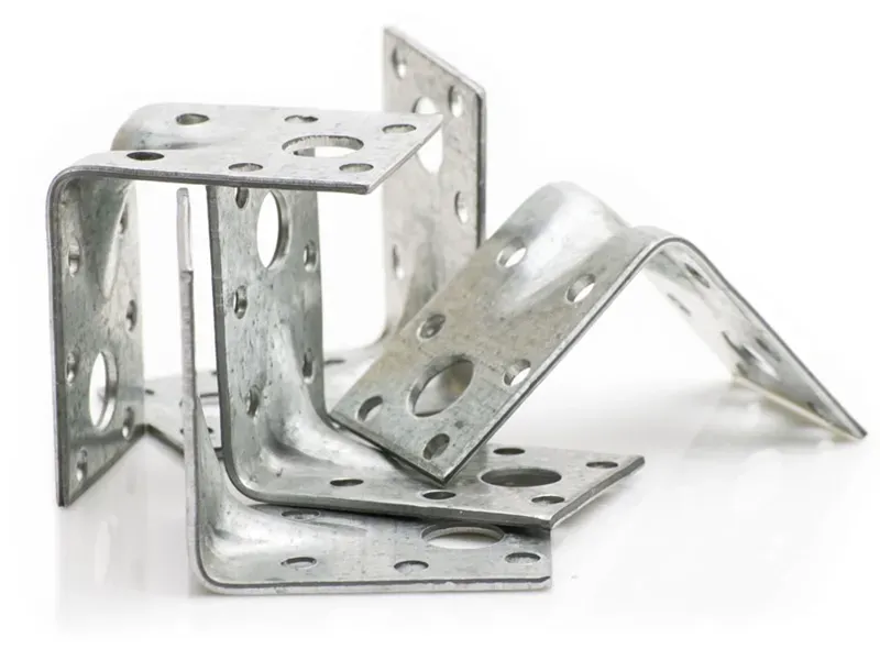
Stamped Brackets
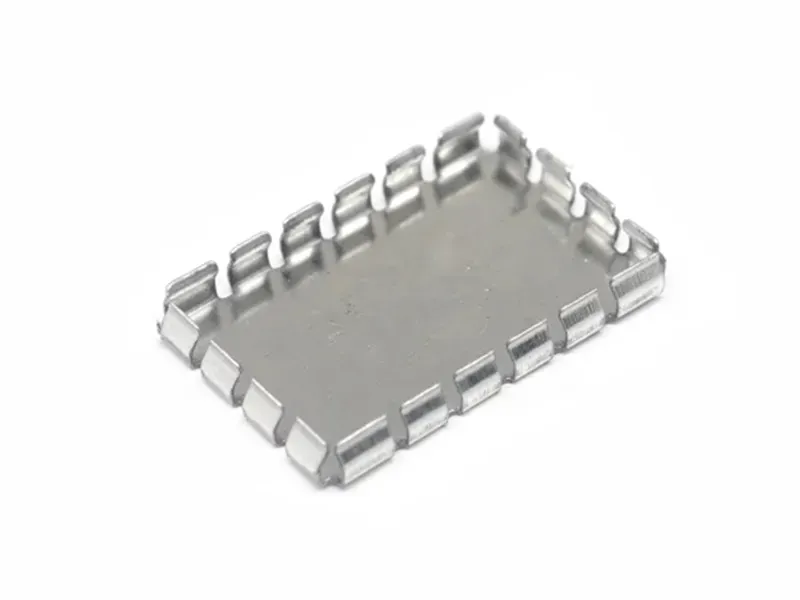
EMI RFI Shield
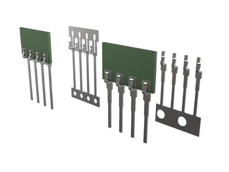
Lead Frame
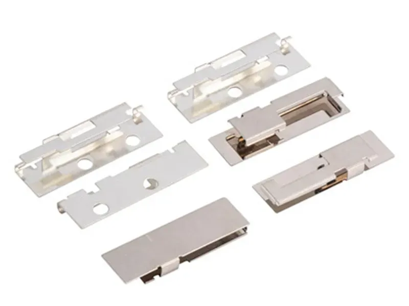
Metal Assemblies
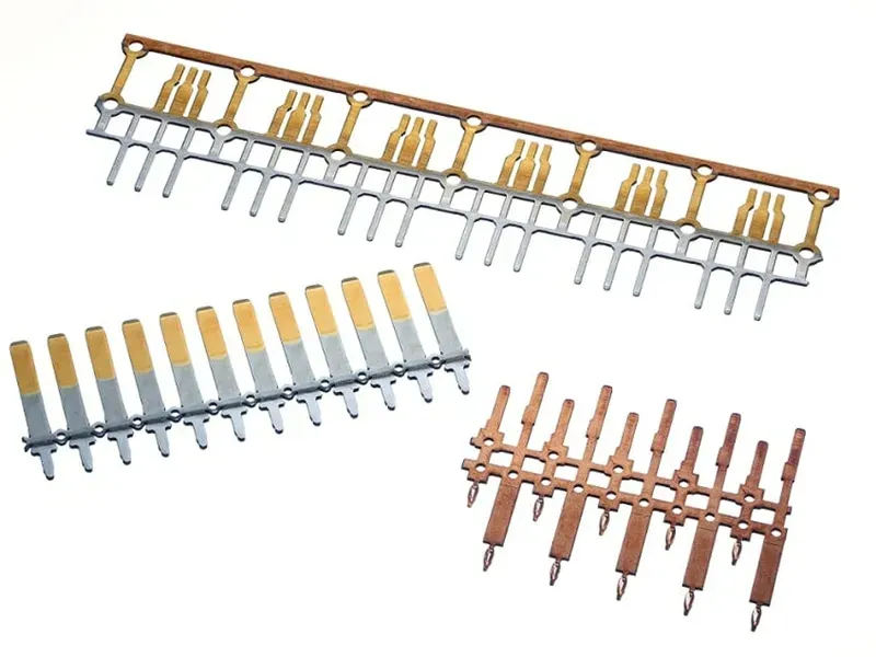
Stamped Electrical Terminals
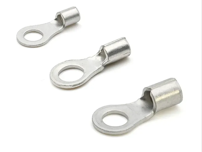
Eyelet Wire Connector
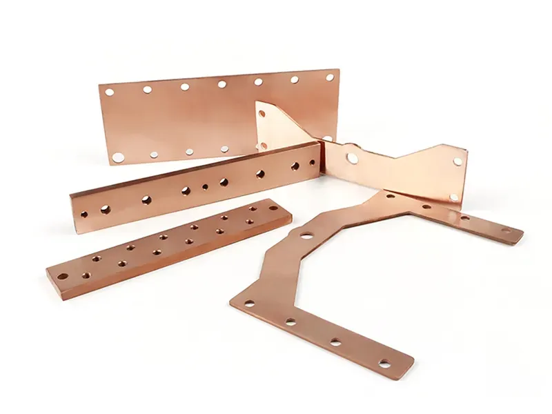
Stamped Busbars
Request DFM EvaluationExplore All ProductsMANUFACTURING CAPABILITIESIntegrated Manufacturing Capabilities
From individual precision metal stamped parts to complex, multi-component stamped metal assemblies, we unify tooling, high-speed stamping, and secondary joining under one roof. Our integrated workflows maximize production efficiency and eliminate supplier fragmentation for Tier 1 OEMs. Our high-speed progressive die stamping lines produce individual stamped components with consistent dimensional accuracy across millions of production cycles, creating a stable baseline for precision assembly.
Request DFM EvaluationWe eliminate secondary handling deviations by integrating complex joining features directly within the stamping cycle or via automated secondary lines. Our production cells are engineered to maintain critical dimensions across millions of cycles, ensuring high repeatability for structural modules.
Automated Joining: Parameter-locked resistance spot welding, automated robotic assembly, and secondary semi-automated lines.
In-Die Automation: High-speed in-die tapping, multi-stage threading, staking, and automated hardware insertion.
Mechanical Interlocking: Orbital riveting, clinch joining, tox locking, stacked laminations, and structural staking.
Stamping Geometry Capabilities: Fine coining, tip coin profiling, countersunk holes, compliant pin (eye-of-the-needle) geometric forming, skiving, and precision embossing.
To safeguard assemblies against environmental corrosion, galvanic degradation, and hydrogen embrittlement, we provide comprehensive industrial surface finishing and post-manufacturing treatments. Every batch undergoes strict quality controls to guarantee uniform adhesion and dimensional stability.
Pre & Post-Plating Lines: Reel-to-reel plating, selective spot plating, barrel and rack plating utilizing copper, nickel, pure tin, tin-lead, silver, gold, and zinc finishes.
Protective Surface Coatings: Electrostatic powder coatings (epoxy, nylon, PVC, polyester, polyurethane), e-coating (KTL), vinyl plastisol liquid dipping, and specialized anti-corrosion geomet coatings.
Mechanical Conditioning: High-cleanliness washing/degreasing, automated deburring, vibratory deflashing, brushing (hairline finish), and micro-polishing.
Metallurgical Enhancement: Controlled atmosphere heat treatment, carburizing, nitriding, and precision stress-relieving.
True multi-component stamped assemblies often require the faultless joining of dissimilar metals, engineered plastics, or specialized fasteners. Our automated hardware insertion cells are fully synchronized to feed and seat standard and custom components without fracturing the parent metal grid.
Mechanical Fasteners: Precision nuts, threaded studs, engineered fasteners, bushings, and custom screw machine parts.
Precision Inserts: High-retention pemserts, self-clinching inserts, metal inserts, and conductive pins.
Hybrid Substrates: Seamless overmolding and insert molding integration, combining stamped profiles with custom plastic pieces and localized insulation modules.
PRODUCT APPLICATIONSIndustries Served
Discover how we translate precision engineering into industry-specific success. From renewable energy to semiconductor processing, our components are tailored to meet rigorous sector standards — backed by documented case studies.
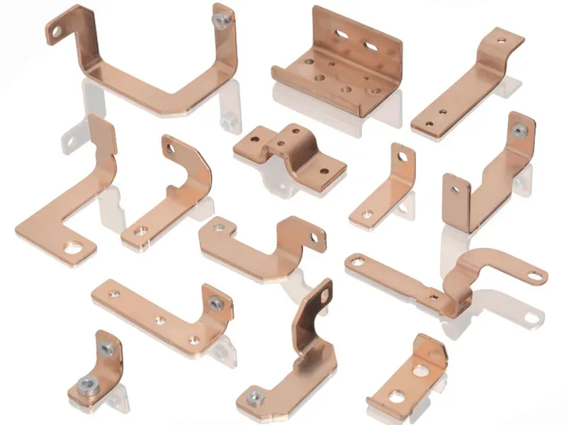
EV Metal Stampings
Learn MorePlastic-Metal Stampings
Learn More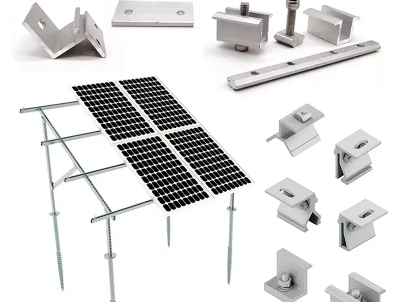
Solar
Learn More
Logistics
Learn More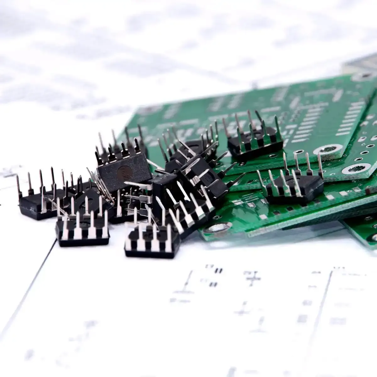
Semiconductors
Learn More
Medical
Learn More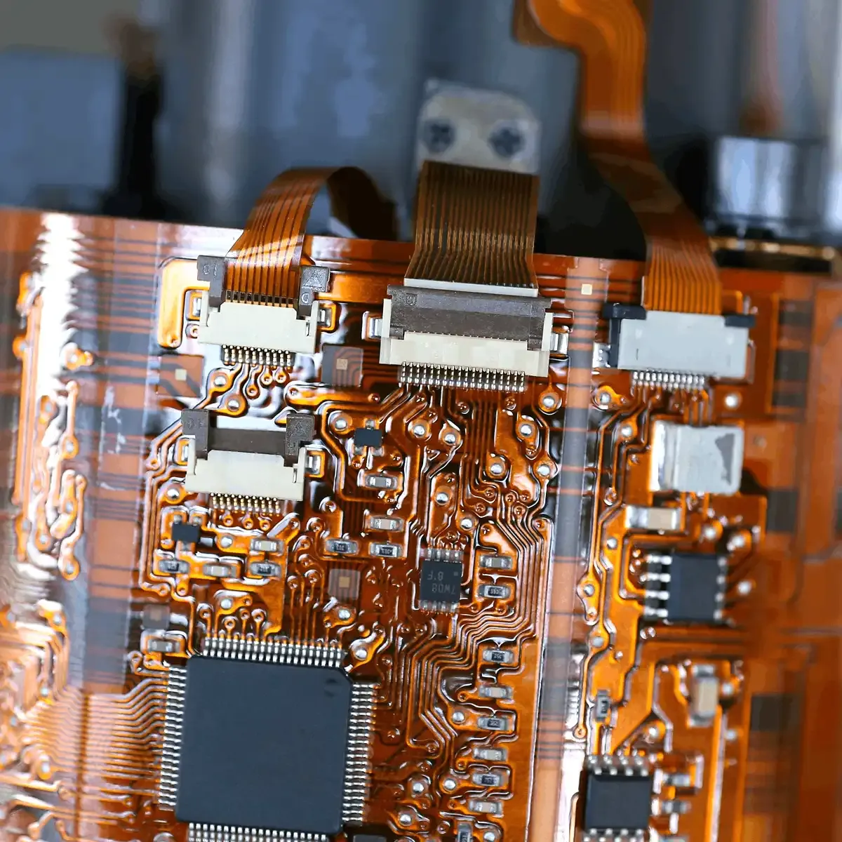
Consumer Electronics
Learn More
Aerospace
Learn More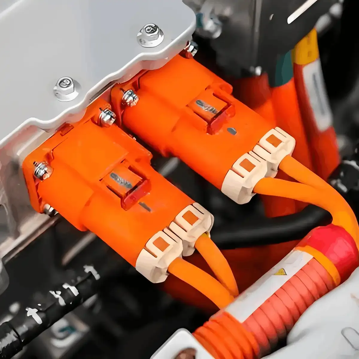
Energy
Learn More
Defense
Learn More- MANUFACTURING CAPABILITIES
Metal Stamping & Die Tooling
Engineered for high-volume reliability and critical automotive tolerances. Leveraging our ultra-precision tooling backbone—powered by simultaneous CNC, Wire EDM, and PG grinding—we build elite high-speed progressive dies and precision compound tooling to guarantee strict ±0.01mm accuracy. Our in-house tool room designs and builds custom progressive die tooling optimized for high-volume assembly production, ensuring long die life and tight tolerances. From heavy-gauge structural brackets to intricate electrical terminals & contacts, we provide a true end-to-end stamping ecosystem. Our unique integrated manufacturing advantage seamlessly bridges pure metal stamping with advanced insert molding operations under one roof, delivering a unified, single-source solution from raw alloy selection to final surface treatment.
Learn More - MANUFACTURING CAPABILITIES
Precision Metal Stamped Parts & Assemblies
Engineered for critical conductivity and uncompromising structural integrity. As an IATF 16949 certified manufacturer, we specialize in high-volume custom precision metal stamping parts that demand strict tolerances. Powered by state-of-the-art 35T and 50T precision presses and a sub-micron in-house tooling ecosystem, we expertly process high-performance copper alloys, stainless steel, and specialty metals. Our capabilities span a comprehensive portfolio, including micro-precision electrical terminals, lead frames, robust stamped metal brackets, and EMI/RFI shields. Moving beyond standard stamping parts manufacturers, we combine these stamped metal components with seamless in-house insert molding integration, delivering true one-stop, zero-defect assemblies for your most complex engineering challenges.
Learn More
Engineering Solutions & Design Insights
Access expert technical guidance to optimize your component designs and resolve manufacturing challenges. Our engineering resources cover critical material selection, tolerance control, and failure prevention to ensure reliable performance in your specific application.
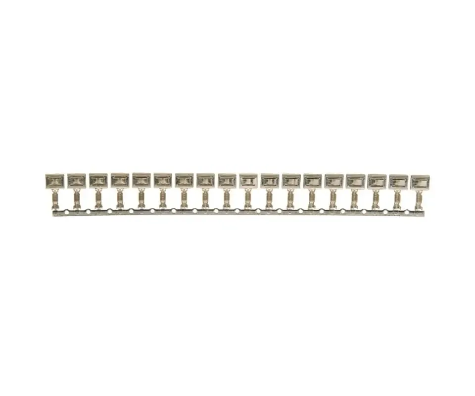
Before Plating Batch: Stamped Electrical Terminals Finish Audit Checklist
A supplier who plates your terminals but skips the JESD201 post-plating anneal will pass the incoming dimensional check. You discover tin whiskers only after field returns arrive. This checklist audits plating specification, pre-treatment protocols, and post-plating verification. Go through every item.
Learn More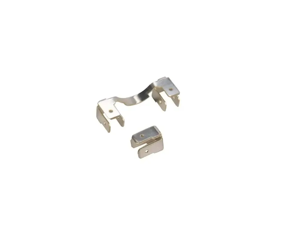
Before PPAP Submission: Stamped Electrical Terminals Compliance Audit Checklist
A PPAP package submitted with a compliance letter but without the Cpk capability study will pass the document checklist and fail the customer SQE review. This checklist audits dimensional capability data, material cert traceability, and testing standards documentation before the submission package leaves your supplier. Go through every document.
Learn More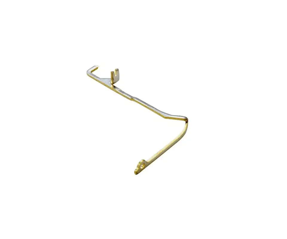
Before Die Design: Stamped Electrical Terminals DFM Readiness Checklist
A terminal drawing that passes CAD review but lacks springback compensation data will drift out of tolerance by stroke 50,000. Your supplier catches it only at first-article rejection. This checklist audits flat blank layout, bend radii, and material grain alignment before die steel is cut. Go through every item.
Learn More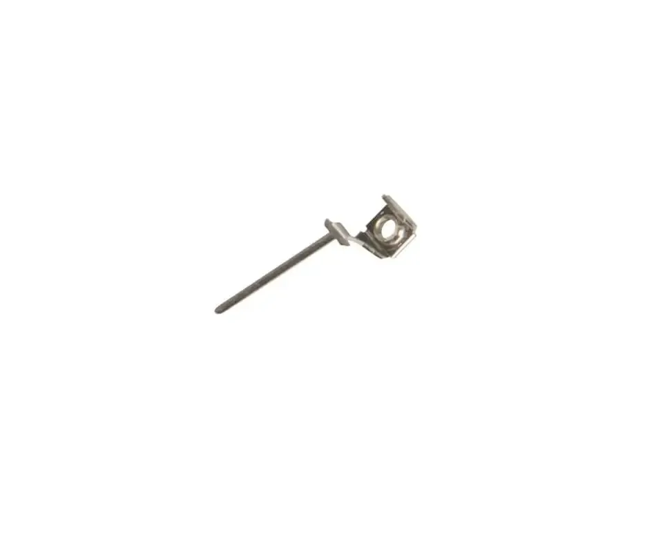
Before Tooling Cut: Stamped Electrical Terminals Supplier Audit Checklist
A missed JESD201 anneal on your terminal lot triggers PPAP rejection, and you catch it only at the compliance audit. This checklist verifies DFM sign-off, material certs, and compliance docs before tooling cut. Go through the full audit.
Learn More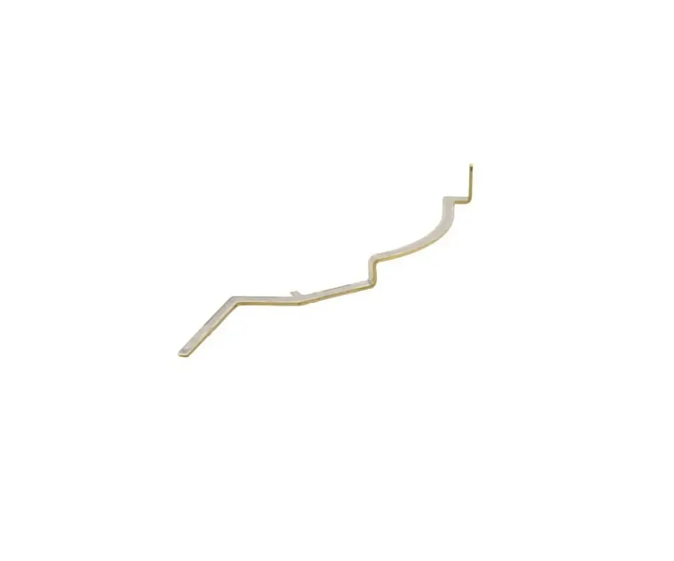
Production-Scale Consistency: Appliances Stamped Electrical Terminals Engineering Guide
A washing machine control board terminal passing factory testing fails after 2,000 cycles when the crimp joint relaxes. In this guide, you will learn cost-optimized material selection and UL 60335 compliance. Read the full guide.
Learn More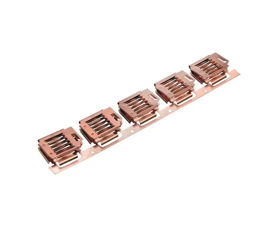
USCAR-Validated: Automotive Stamped Electrical Terminals Engineering Guide
An ECU stamped terminal passing testing at 25°C fails after 1,000 thermal shock cycles from -40°C to +125°C. In this guide, you will learn USCAR-2 contact stability and IATF 16949 PPAP. Read the full guide.
Learn MoreSERVICES LIBRARYExplore Other Industrial Metal Stamping Services Available
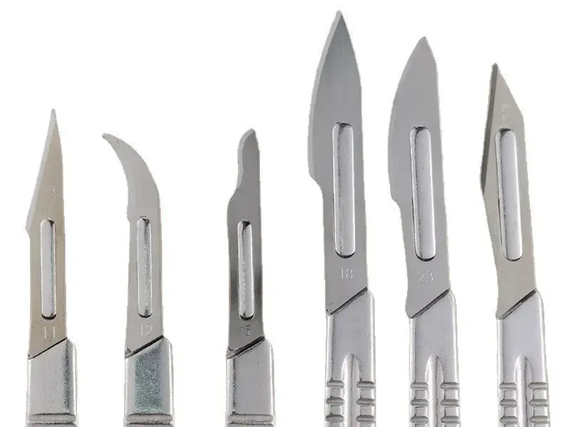
Medical Metal Stamping
High-speed medical stamping and insert molding with micro-tolerances down to ±0.005 mm. Processing Titanium, BeCu, and SS for scalable, cleanroom-ready parts.
Learn More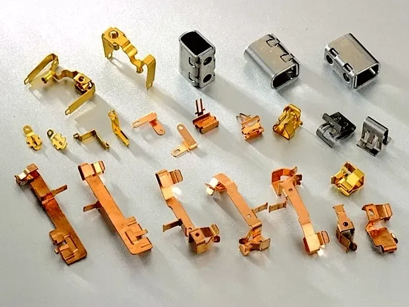
Appliances Metal Stamping
High-volume precision stamping for the appliance industry. Offering progressive die stamping, insert molding, and automated assembly with ±0.02mm tolerances for over 500 million parts annually.
Learn More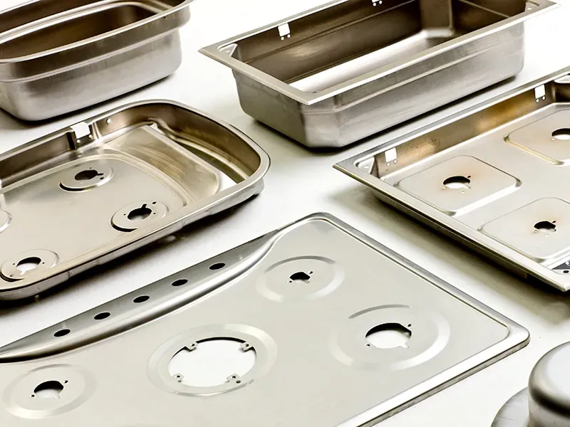
Consumer Goods Metal Stamping
Consumer brands require flawless aesthetics at high-volume production scales. Our progressive metal stamping delivers consistent quality and cost efficiency.
Learn MorePlastic-Metal Stampings
High-volume automotive metal stamping and precision insert molding. Delivering zero-defect EV and chassis components with 45T-800T capacity and up to 1,000 SPM speeds.
Learn MoreRequest DFM EvaluationAccess Industry DatabaseTECHNICAL REFERENCEFrequently Asked Questions
Answers to common questions regarding precision, tooling, materials, and our integrated molding capabilities.We utilize ISO Class 7 cleanrooms and multi-stage ultrasonic cleaning systems to eliminate microscopic particulates, followed by vacuum-sealed packaging to ensure components remain contamination-free during transit and assembly.
Our high-speed progressive stamping processes consistently maintain precision tolerances as tight as ±0.002mm, meeting the extreme dimensional stability requirements for wafer handling and automated lithography equipment infrastructure.
We utilize specialized carbon-fiber-reinforced and conductive-additive resins with verified surface resistivity testing to provide permanent static dissipation, preventing electrostatic discharge damage in sensitive electronic production environments.
Yes, we specialize in high-temperature injection molding for PEEK, PFA, and PVDF, employing advanced thermal control units to ensure material purity and chemical resistance for aggressive fluid delivery systems.
We employ a validated four-stage ultrasonic degreasing and chemical passivation process to eliminate all trace oils and metallic particulates, ensuring outgassing levels comply with high-vacuum semiconductor specifications.
As an IATF 16949-certified manufacturer, we provide comprehensive metallurgical and resin traceability reports, including Certificate of Conformity (CoC) and chemical analysis for every individual production lot.
Our engineering team performs sub-micron DFM analysis to identify stress points and simplify complex geometries, optimizing mold cavitation and stamping sequences to maximize yield and reduce unit costs.
We recommend SS316L or Hastelloy for stamped components and high-purity PFA for molded parts, as these materials offer superior corrosion resistance against aggressive etching precursors and precursors.

Still have questions?
Our engineering team loves solving complex problems. Chat with us or send your drawing for a review.
Request DFM EvaluationReady to Manufacture With One Accountable Factory?
From in-house tooling to high-volume production — stamping, molding, plating and assembly under one IATF 16949 roof. Send your spec and volume, get a quote within 24 hours.