
Ultra-Precise Tin Plating Turnkey Solutions
Overcoming critical electrochemical and metallurgical challenges such as macro-thickness variance across complex stamped terminals and long-term tin whisker proliferation, we engineer high-purity tin layers optimized for reliable solderability and excellent corrosion resistance. By deploying advanc…
Overcoming critical electrochemical and metallurgical challenges such as macro-thickness variance across complex stamped terminals and long-term tin whisker proliferation, we engineer high-purity tin layers optimized for reliable solderability and excellent corrosion resistance. By deploying advanced inline heat treatments and maintaining precise control over electrolyte chemistry and localized current density, our workflows transform raw copper or brass alloy substrates into highly stable conductive pathways suitable for high-density power distribution assemblies. Backed by our rigorous IATF 16949-certified quality framework, we precisely modulate deposition parameters to guarantee a highly uniform coating thickness distribution, thereby eliminating micro-structural defects and ensuring zero-failure electrical performance under rigorous engineering specifications.
Superior Solderability: Enhanced wetting for reliable electrical connections.Whisker Mitigation: Specialized annealing prevents internal short circuits.High Conductivity: Optimal current flow for precision power terminals.Corrosion Resistance: Reliable protection against oxidation and humidity.Request DFM Evaluation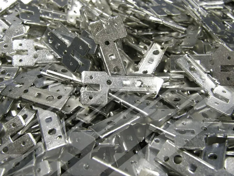
What is Tin Plating & The Engineering Logic Behind It
Tin plating is a specialized electrochemical process that deposits a high-purity metallic tin layer onto copper, brass, or steel substrates. Unlike general protective coatings, tin is primarily utilized for its exceptional solderability, low contact resistance, and non-toxic properties. This finish provides a critical conductive interface, preventing oxidation of the base metal while ensuring reliable electrical connectivity for high-density PCB terminals, battery connectors, and power distribution busbars.
Precision Pre-treatment & Activation
Raw components undergo multi-stage ultrasonic degreasing and electrolytic cleaning to eliminate residual lubricants from the stamping or machining process. This is followed by a micro-etching phase to strip oxide layers and activate the substrate surface. This meticulous preparation ensures an atomic-level bond between the tin and the base metal, preventing future peeling or solder failure during assembly.
Controlled Electro-deposition
The activated parts are immersed in a high-stability methanesulfonic acid or alkaline electrolyte bath. By precisely modulating current density and bath temperature, tin ions are uniformly deposited across the component’s geometry. Our automated lines maintain tight control over grain structure, allowing us to deliver either a “Matte” finish for superior solderability or a “Bright” finish for enhanced aesthetic and wear resistance.
Anti-Tarnish & Heat Treatment
To ensure long-term shelf life, components undergo a specialized neutralization and anti-tarnish dip to prevent yellowing or oxidation. For critical electronic applications, we implement a post-plating baking cycle (annealing). This vital step relieves internal stress within the tin layer, significantly mitigating the risk of “Tin Whisker” growth which could otherwise cause catastrophic short circuits in fine-pitch components.
Solderability & Quality Verification
Every batch is validated through rigorous outbound inspection protocols. Beyond non-destructive X-ray Fluorescence (XRF) thickness testing, we perform “Steam Aging” and dip-and-look solderability tests to simulate long-term storage conditions. This guarantees that your components strictly adhere to IPC and MIL-STD specifications, ensuring 100% wetting performance during your downstream soldering processes.
Engineered Tin Plating Specifications & Capabilities
Kravzik provides rigorous process control to ensure consistent, repeatable results for electronic and industrial applications. Our tin plating capabilities are calibrated to meet the tight dimensional tolerances and performance criteria required for precision electrical terminals, battery busbars, and high-density PCB connectors.
Request DFM EvaluationPlating Classifications
Bright Tin (Low-friction/Aesthetic) & Matte Tin (Superior Solderability). Fully compliant with ASTM B545 and MIL-T-10727 standards.
Coating Thickness
Standard: 2.5µm – 20µm (0.0001″ – 0.0008″). Custom heavy-build tinning available for high-current power distribution components.
Dimensional Tolerance Control
±0.002mm (2µm) — ensuring precision fit for micro-stamped terminals, press-fit pins, and tight-tolerance machined housings.
Environmental Endurance
Exceeds 96-168 hours in neutral salt spray testing (ASTM B117) when utilized with specialized anti-tarnish post-treatment cycles.
Solderability Assurance
100% Wetting Balance verified per IPC-J-STD-003. Guaranteed 12-month shelf life under standard controlled storage conditions.
Whisker Mitigation (Stress Relief)
Integrated post-plating baking (150°C for 1-2 hours) to minimize internal compressive stress and prevent catastrophic tin whisker growth.
Compatible Substrates for Precision Tin Plating
The long-term reliability and solderability of a tin finish depend heavily on the metallurgical interaction between the tin layer and the base metal. Kravzik engineers utilize specialized underplating strategies and activation protocols to manage intermetallic compound (IMC) growth and prevent base-metal migration, ensuring a high-performance surface for critical electronic and industrial applications.
Copper & High-Conductivity Alloys (C1100, C1020)
The industry standard for power busbars and high-current connectors. To prevent the natural diffusion of copper into the tin layer—which creates brittle intermetallic compounds—we implement a precision Nickel barrier underplate. This metallurgical “block” preserves the purity of the surface tin, ensuring the component maintains 100% solderability and low contact resistance even after extended shelf life.
Brass & Phosphor Bronze (C2680, C5191, C3604)
Extensively used for micro-stamped terminals and spring-loaded contacts. These alloys contain zinc, which can migrate to the surface and cause rapid oxidation of the tin finish. Our process utilizes a dense, low-stress Nickel undercoating to seal the substrate, effectively neutralizing zinc migration and preventing the “yellowing” or loss of conductivity common in lower-tier plating operations.
Cold-Rolled & Mild Steel (SPCC, 1008, 1010)
Ideal for EMI/RFI shielding cans and battery hardware requiring high structural integrity. Tinning steel requires aggressive oxide removal and a high-efficiency Copper or Nickel strike to ensure a pore-free deposit. Our automated line monitors bath chemistry to provide a dense, non-porous tin layer that delivers excellent corrosion protection and a reliable ground path for sensitive electronics.
Stainless Steel Series (SUS304, SUS316)
Frequently specified for medical device components and food-grade electrical interfaces. Due to the high-chromium passive layer, stainless steel is notoriously difficult to plate. We employ a specialized “Woods Nickel Strike” to penetrate the passive film and create a high-strength metallurgical bond, allowing for a uniform tin topcoat that will not peel or flake under mechanical stress.
Aluminum Alloys (6061-T6, 7075)
Used in lightweight aerospace heat sinks and power distribution blocks. The primary challenge is the rapid formation of aluminum oxide which compromises adhesion. Our multi-stage process includes double-zincate immersion followed by a Copper or Nickel underplate, providing a stable foundation that allows the tin layer to achieve maximum adhesion and thermal conductivity.
Essential Design Guidelines & Process Limitations
Proactive design optimization prevents assembly failures and ensures your components meet exact engineering specifications for electrical performance. Consider these critical geometric and metallurgical factors before finalizing your CAD models for the tin electroplating process.
Tin electroplating adds a definitive layer of material—typically ranging from 2.5µm to 15µm (0.0001″ to 0.0006″)—to every surface of your component. Because internal and external threads experience dimensional changes up to four times the plating thickness on their pitch diameter, Kravzik engineers recommend specifying pre-plate allowances or utilizing slightly oversized taps for fine-threaded connectors to guarantee smooth mechanical assembly and electrical mating.
Like all electrolytic processes, tin deposition relies on electrical current density, which is subject to the “Faraday cage” effect. Deep blind holes, narrow channels, and complex inner diameters will naturally receive a thinner coating than exterior edges. For critical electrical contacts inside recessed geometries, we advise designing auxiliary drainage/access holes or consulting with our team to optimize part orientation and anode placement during the plating cycle.
When plating tin directly over copper or brass, a natural diffusion occurs that creates intermetallic compounds (IMC), which can compromise solderability over time. To ensure a 12-month shelf life and reliable wetting, we recommend a 1.25µm–2.5µm Nickel underplate. Designers must account for this additional stack-up thickness in high-precision electronic assemblies to prevent interference fits in press-fit pin applications.
In high-density electronic packaging, the spontaneous growth of “tin whiskers” poses a severe risk of electrical short circuits. Our process includes a mandatory post-plating bake (annealing) for critical components to relieve internal compressive stress. Please notify our engineering team of your minimum spacing requirements so we can mandate the appropriate thermal cycles and grain structure controls to safely mitigate whisker risks.
VISUAL EXCELLENCEData-Driven Showcase: Engineered Tin Finishes
The final functional performance of a tin-plated component is dictated by its grain structure and organic additive levels. Explore our standard tinning profiles to identify the precise technical specifications and surface morphology required for your specific soldering or electrical contact assembly.
ELECTROLYTIC FINISHHigh-Luster Bright Tin
RoHS CompliantLow FrictionAesthetic FinishHigh ConductivityOur bright tin process utilizes specialized organic brighteners to produce a highly reflective, aesthetically pleasing surface. Beyond its visual appeal, the fine-grained structure provides a lower coefficient of friction, making it ideal for connector housings and pluggable interfaces where insertion force must be minimized while maintaining excellent atmospheric corrosion resistance.
Grain StructureFine-grained with organic brightenersSolderabilityExcellent (Immediate wetting)Visual AppearanceHigh-gloss, mirror-like silverPrimary BenefitLow insertion force and decorative appealIdeal For:Consumer electronics, decorative hardware, pluggable connectorsINDUSTRIAL FINISHPure Matte (Dull) Tin
Whisker ResistantSuperior SolderabilityHigh TemperaturePure DepositSpecifically engineered for high-reliability electronics, our matte tin finish is free of organic brighteners, resulting in a larger grain size that significantly reduces internal compressive stress. This morphology is the industry standard for preventing tin whisker growth and ensuring the highest possible solderability performance, even after aggressive thermal aging or long-term storage.
Purity Level>99.9% Pure Metallic TinWhisker RiskMinimized (Low internal stress)Surface TextureNon-reflective, satin/matte grayPrimary BenefitMaximum solderability and whisker mitigationIdeal ForPCB terminals, semiconductor leads, high-density SMT componentsSPECIALTY THERMAL FINISHReflowed / Hot-Dip Style Tin
Zero PorosityUltra-SmoothExtended Shelf LifePremium DefenseBy subjecting electroplated tin to a controlled induction or oil-bath reflow cycle above its melting point (232°C), we create a "flow-melted" surface. This process eliminates porosity and creates a dense, fused layer with a controlled intermetallic base. It provides the absolute highest level of corrosion protection and maintains solderability for years, exceeding the performance of standard electro-deposition.
Surface RoughnessRa < 0.4 μm (Ultra-smooth)PorosityNear-zero (Fused metallic layer)Shelf Life24+ Months (In controlled environments)Primary BenefitSuperior environmental sealing and densityIdeal ForCritical power grid components, automotive fuse rails, maritime electronics Request DFM EvaluationView Surface Treatment SolutionsSERVICES LIBRARYExplore Other Industrial Surface Treatment & Finishing Services Available
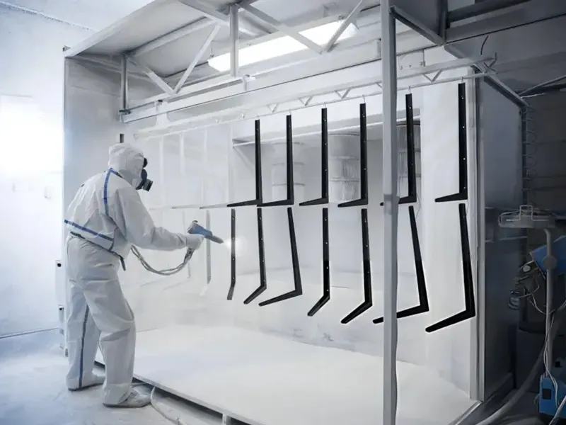
Powder Coating
Eliminate surface defects like orange peel on complex geometries. Our automated lines guarantee 1000h salt spray resistance for heavy-duty industrial components.
Learn More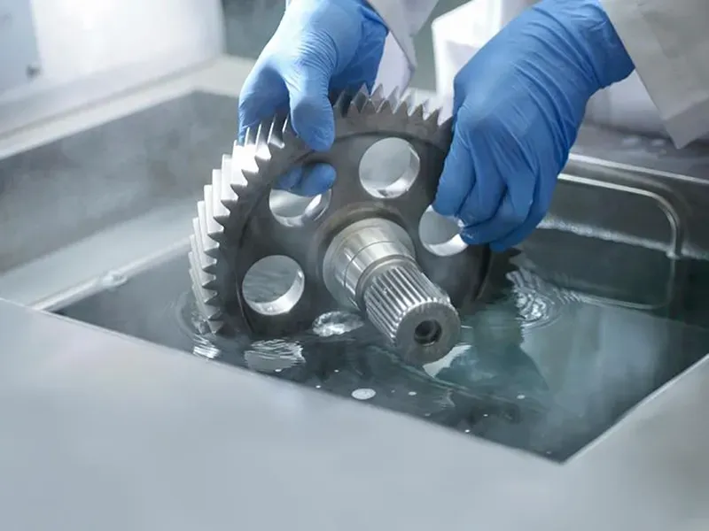
Degreasing
Eliminate microscopic contaminants that ruin precision plating. Achieve >40 dynes/cm surface energy for flawless secondary processing.
Learn More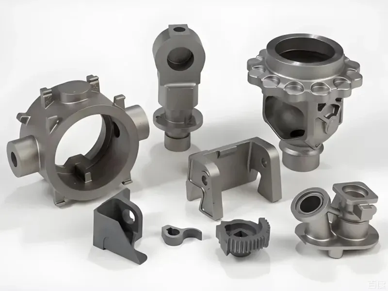
Nitriding
Forget brittle surfaces and dimensional warping. Kravzik delivers 1200 HV surface hardness while maintaining absolute ±5µm geometric precision.
Learn MoreRequest DFM EvaluationSee More Surface TreatmentTECHNICAL REFERENCEFrequently Asked Questions
Answers to common questions regarding precision, tooling, materials, and our integrated molding capabilities.We maintain 100% wetting balance per IPC-J-STD-003 standards. Every batch undergoes steam aging and dip-and-look testing to validate surface activity and oxide-free performance for critical high-density electronic assemblies.
We implement mandatory post-plating thermal annealing at 150°C. This process relieves internal compressive stress within the tin lattice, significantly reducing the risk of spontaneous whisker formation and preventing catastrophic electrical short circuits.
Yes, we highly recommend a 1.25µm–2.5µm nickel barrier. This undercoat prevents copper diffusion into the tin layer, which creates brittle intermetallic compounds that compromise solderability and mechanical bond strength over time.
Our automated plating lines achieve a precise coating tolerance of ±2µm. This ensures perfect mechanical fit for micro-stamped terminals, press-fit pins, and tight-tolerance housings without compromising the electrical contact integrity.
Matte tin is ideal for superior solderability and whisker mitigation in electronics. Bright tin offers a lower coefficient of friction and better aesthetics, making it preferred for pluggable connector housings and high-visibility industrial hardware.
Absolutely. All our electrolytes and post-treatment anti-tarnish solutions are 100% lead-free and hexavalent chromium-free. We provide full material certification to support your environmental compliance and global supply chain requirements.
Yes, we utilize a specialized Woods Nickel Strike pre-treatment. This aggressively penetrates the passive chromium-oxide layer of stainless steel, creating a high-strength metallurgical bond that prevents the tin coating from peeling or flaking under mechanical stress.
We guarantee a minimum 12-month solderability shelf life under controlled storage conditions. By utilizing advanced anti-tarnish dips and precision grain structure control, we preserve surface activity and prevent the oxidation often seen in standard plating.

Still have questions?
Our engineering team loves solving complex problems. Chat with us or send your drawing for a review.
Request DFM EvaluationReady to Manufacture With One Accountable Factory?
From in-house tooling to high-volume production — stamping, molding, plating and assembly under one IATF 16949 roof. Send your spec and volume, get a quote within 24 hours.