
Engineering Guide
EMI Shield Manufacturing: Stamping vs Etching vs Laser vs CNC
Table of Contents
A telecom program shipped its RF shield redesign to laser cutting because the prototype shop had a laser and the quote was fast. At 400,000 pieces a year the laser route landed at USD 0.31 per shield against a stamping quote of USD 0.07 — a USD 96,000 annual delta — and the laser-cut edges carried a 12 µm recast layer that failed the adhesion test for the nickel-plating spec. The program burned three weeks requalifying a new supplier.
The reverse mistake is just as common. A defense prototype order of 800 shields went to progressive die tooling at USD 24,000 because the buyer "always used stamping." The shields shipped six weeks later than the program needed, and the die sat idle after the order — a 30:1 tooling-to-part spend that no one had challenged.
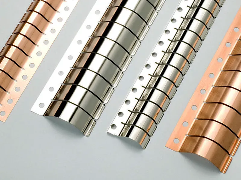
EMI shields look like simple sheet-metal parts: a can, a frame, a clip, a finger. In a 5G base station or an automotive ECU, that small stamped shell is the difference between passing CISPR 25 and re-spinning the board. The four manufacturing routes — progressive die stamping, chemical etching, laser cutting, and CNC machining — produce shields with different tolerances, different edges, and radically different cost curves. Choosing the wrong one costs money, plating failures, and qualification delays.
This guide compares the four processes on the numbers that matter, and maps each shield architecture to its natural process.
The Snapshot
- Progressive die stamping is the production standard for shield cans and frames: ±0.05 mm typical, up to 800 SPM, USD 0.03 – 0.15 per part at volume.
- Chemical etching suits thin, fine-feature shields (0.05 – 0.25 mm) at low volume: no tooling, ±0.025 mm typical, but per-piece cost 2 – 4 times stamping.
- Laser cutting wins for prototypes and complex contours but leaves a recast layer and heat-affected zone that plating must be qualified against.
- CNC machining is for thick, machined housings (1 – 10 mm) where EMI gaskets and threaded inserts justify the cost — never for thin cans.
- The volume crossover between etching and stamping sits near 20,000 – 50,000 pieces (typical); above it, stamping wins by 2 – 5 times.
How the Four Processes Work
Progressive die stamping feeds a coil through a multi-station die: pierce, blank, form, coin, and cut-off in one pass at up to 800 SPM. The shield is defined by hardened steel, so tolerance, form, and burr direction are locked in for millions of strokes. This is the route for anything that ships in quantity.
Chemical etching exposes a photoresist pattern and dissolves unprotected metal from both sides. It is tooling-free — the pattern is artwork — and it handles very thin stock and dense hole patterns that would buckle a die. The edge is rounded and stress-free, and there is no burr by nature.
Laser cutting melts or ablates the contour with a focused beam, typically a fiber laser on sheet up to 2 – 3 mm. It is the fastest route to a new geometry — no die, no artwork — and it cuts complex curves that stamping would split into several stations. The trade-off is a recast layer and heat-affected zone on the cut edge, and a slower cycle than stamping by an order of magnitude.
CNC machining mills the shield from billet or plate. It is the only route that produces thick, stiff, machined housings with threaded holes and sealing faces — think aluminum ECU enclosures, not thin cans. At 1 – 10 mm wall thickness it has no competitor, but for thin shields it is economically absurd.
| Feature | Stamping | Etching | Laser | CNC |
|---|---|---|---|---|
| Typical thickness | 0.08 – 4.0 mm | 0.025 – 0.25 mm | 0.1 – 3.0 mm | 1 – 10 mm |
| Tolerance (typical) | ±0.05 mm | ±0.025 mm | ±0.1 mm | ±0.01 mm |
| Tooling cost | USD 8k – 60k | Near zero | Zero (program) | Zero (program) |
| Lead time to first part | 3 – 5 weeks | 1 – 2 weeks | Days | Days – weeks |
| Throughput | Up to 800 SPM | Batch panels | 10 – 60 pcs/min | Minutes per part |
| Edge condition | Shear + burr (controlled) | Rounded, burr-free | Recast layer + HAZ | Machined, chip-free |
| Unit cost at 100k/yr | USD 0.03 – 0.15 | USD 0.08 – 0.30 | USD 0.15 – 0.40 | USD 1.50 – 8.00 |
Tolerance and Edge Quality
Tolerance is the first thing engineers compare, and it is the easiest to misread, because each process quotes a number with a different meaning behind it.
Stamped tolerance is die-locked. A precision-ground progressive die holds form and apertures to ±0.05 mm typical, with springback compensated in the tool steel. The number does not drift with operator skill or material lot; it drifts only with die wear, which is measured and corrected on a maintenance schedule. Coined features — dimples, standoffs, contact bumps — are formed in the same pass, so the shield's mechanical interfaces repeat at stroke one million exactly as they did at stroke one.
Etched tolerance is chemistry-locked. The etchant removes material laterally while cutting through thickness, so the as-etched aperture is wider than the artwork by the etch factor — typically 1.5 to 2.5 times the etch depth per side, depending on etchant temperature and agitation. The supplier compensates in artwork, but the compensation is a process variable: if etch rate drifts, the aperture drifts. Real-world etching holds ±0.025 mm typical, which is tighter than stamping on paper — but the tolerance is on a flat, unformed part, and there is no coined geometry to hold.
Laser tolerance is machine-locked. A modern fiber laser with a linear drive holds ±0.1 mm typical on contours, which is loose compared with the other three. More important than the number is the edge: the beam melts a recast layer 5 – 20 µm deep (typical) and leaves a heat-affected zone beside it. That metallurgical change is invisible on a CMM report but decisive at the plating tank.
CNC tolerance is the tightest — ±0.01 mm typical — because it is cutting with a rigid tool and probing in-process. But the tolerance costs time: a machined shield takes minutes per part, and the unit price reflects it.
The practical ranking for a thin shield can: stamping for production repeatability, etching for flat fine-feature parts, laser for iteration speed, CNC only when the part is thick or machined-featured.
Material and Shielding Performance
All four processes can cut the same shield materials; the differences show up in how the material behaves at the edge and in the form.
| Material | Conductivity | Stamping | Etching | Laser | CNC |
|---|---|---|---|---|---|
| Brass (C260/C268) | ~28% IACS | Excellent | Good | Good | Good |
| Nickel silver | ~5 – 8% IACS | Excellent | Good | Good | Fair (work-hardens) |
| Stainless 301/304 | ~2.5% IACS | Excellent (spring temper) | Good | Excellent (laser-friendly) | Good |
| Copper C1100 | ~101% IACS | Excellent | Excellent | Good (reflectivity) | Excellent |
| Tin-plated steel | ~10% IACS | Excellent | Poor (plating interferes) | Fair | Good |
| Aluminum | ~61% IACS | Good (bend limits) | Poor (etch control) | Excellent | Excellent |
Shielding effectiveness at a given frequency is driven by conductivity, thickness, and apertures — not by the forming process. A 0.2 mm brass can shields roughly as well as a 0.2 mm brass can regardless of how the edges were cut; the process differences are mechanical and metallurgical at the edge, not bulk shielding. What the process does change: whether the material can be formed into a can with coined standoffs (stamping), whether a fine vent array is economical (etching), whether the edge survives plating adhesion (stamping and CNC yes, laser needs qualification), and whether thin soft copper can be handled at all (etching).
Skin depth is worth keeping in view. At 1 GHz, skin depth in copper is about 2 µm, in brass about 4 µm, and in nickel silver about 10 µm — which is why shield thickness is rarely a shielding problem above a few tens of microns, and why form, grounding, and apertures dominate real-world shielding performance. Choose the material for conductivity and cost; choose the process for geometry, volume, and edge.
When Stamping Wins
Progressive die stamping is the default production route for shield cans, frames, clips, and fingers. Choose it when:
- Volume is real. Above roughly 20,000 – 50,000 pieces per year, the die amortizes and stamping wins on unit cost by 2 – 5 times (typical). At telecom and automotive volumes — 100k to millions per year — there is no contest.
- You need consistent form and aperture. Stamped shields hold ±0.05 mm typical, with springback compensated in the die. Contact fingers, dimples, and standoffs are coined in the same pass, so the shield snaps onto the PCB the same way every time.
- You want plating-ready edges. With burr controlled below 15 µm (typical) and oriented away from functional faces, the stamped edge plates cleanly and passes adhesion tests without requalification.
- Material is standard sheet. Brass, nickel silver, stainless (301/304), copper alloys, and tin-plated steel all stamp cleanly in 0.08 – 4.0 mm.
- You want one supplier for the whole shield family. A single factory with in-house tooling builds the can, the frame, and the clips in one program, keeping PPAP documentation under one roof.
Stamping also wins on the hidden metric: repeatability. A die produces the same part at stroke one and stroke one million; a laser or etch process drifts with its consumables. For shields that must pass CISPR 25 on every build, that repeatability is the qualification itself.
When Etching Wins
Choose chemical etching for the shield cases where a die cannot deliver:
- Very thin stock. Below 0.08 mm, stamping edge quality degrades and etching becomes the practical route — fine for flexible shields and thin RF gaskets.
- Dense, fine apertures. A ventilation pattern with hundreds of small holes, or a fine finger array, is etch-friendly: the pattern is artwork, not a die station.
- Prototypes and pre-production. First-article shields in 1 – 2 weeks from artwork, with the same alloy and geometry as production, let you validate the design before tooling.
- Low volume with no tooling budget. Below the crossover, etching avoids the die entirely — the unit price is higher but the program cost is lower.
The honest limit: etching gives up the coined features. Dimples, standoffs, and stiffening ribs that a die coines in one stroke must be formed in a secondary operation on an etched part. If your shield relies on coined geometry, etching adds process steps instead of removing them.
When Laser Cutting Wins
Laser cutting is the prototyping and low-volume workhorse. Choose it when:
- You need parts in days, not weeks. A new shield geometry can be cut the same day the CAD file lands — no die, no artwork, no waiting.
- The contour is too complex for a simple die. Intricate cutouts, tight radii, and asymmetric shapes that would need a multi-station progressive die can be cut in one pass.
- You are iterating. Design-for-EMI is iterative; the second revision costs only a new program, not a die modification.
The trade-offs are real. Laser-cut edges carry a recast layer and a heat-affected zone, typically 5 – 20 µm deep (typical), which changes plating adhesion and corrosion behavior — the plating spec must be requalified on laser-cut edges. Cycle time is 10 – 60 parts per minute at best, one to two orders of magnitude below a stamping press, and unit cost reflects it. Use laser for development and bridge quantities, then transfer to stamping for production.
When CNC Machining Wins
CNC machining is not a shield-can process; it is a shield-housing process. Choose it when:
- The part is thick and structural. Aluminum ECU housings, chassis plates, and sealed enclosures at 1 – 10 mm wall thickness are machined, not stamped.
- You need machined features. Threaded inserts, sealing faces, gasket grooves, and standoffs are milled in — impossible to coin in thin sheet.
- The volume is low and the spec is tight. Aerospace and defense housings at hundreds to thousands of pieces per year justify machining at ±0.01 mm with full traceability.
For thin shields, CNC is the wrong tool by an order of magnitude — machining a 0.2 mm can costs 10 – 50 times a stamped one and adds nothing the customer can measure.
The Hidden Trade-offs
Four trade-offs hide beneath the process comparison, and each has burned a program.
1. Edge metallurgy decides plating fate. A stamped shear edge and a laser recast edge plate differently. Adhesion, porosity, and salt-spray performance all shift with the edge condition. If the shield is nickel-plated for corrosion (typical: 2 – 8 µm nickel), qualify the plating on the actual production edge — a laser prototype that passes adhesion is not evidence that laser production will.
2. Springback is a stamping variable, not a laser variable. Stamped forms need die compensation for springback; etched and laser parts are flat by nature. A shield with a critical contact angle is easier to get right the first time in etching or laser — and cheaper to repeat in stamping once the die is tuned.
3. The crossover is a band, not a line. The 20,000 – 50,000-piece crossover shifts with part complexity, material, and secondary operations. Model both quotes at your actual annual volume and at a 2-year horizon, including plating and any post-forming.
4. Secondary operations change the comparison. A shield that needs a coined standoff (stamping advantage), a fine aperture array (etching advantage), or a sealed face (CNC advantage) drags the comparison toward the process that makes the dominant feature. Price the whole route, not the blank.
| Shield architecture | Natural process | Why |
|---|---|---|
| Board-level can, 100k+/yr | Stamping | Volume economics, coined standoffs, repeatability |
| Board-level can, prototype | Laser or etching | Days lead time, no tooling |
| Thin RF gasket / finger array | Etching | Thin stock, fine features |
| Frame with dense vent pattern | Stamping or etching | Die if volume, etch if fine pitch |
| Aluminum ECU housing | CNC | Thick walls, threads, sealing faces |
| Clip / spring finger | Stamping | Coined spring geometry, high volume |
The Prototype-to-Production Transition
Most shield programs do not need to choose one process forever — they need a transition plan. The cleanest pattern is laser or etching for development, then stamping for production, with the hand-off managed deliberately.
Phase 1 — Development (laser or etching). The design is still moving: aperture sizes, finger counts, and grounding geometry change as the first CISPR measurements come back. Laser gives same-day parts and zero tooling cost per revision; etching gives flat, burr-free parts that behave closer to the production geometry when the shield is thin. The goal is not cheap parts — it is fast, valid iterations.
Phase 2 — Qualification (match the production process early). The trap is qualifying on laser parts and then discovering the stamped edge plates differently. Run the qualification batch on the intended production process as soon as the design freezes: same material, same thickness, same plating. This is where edge metallurgy, burr orientation, and form repeatability get locked down. A shield that passes CISPR 25 with a laser edge and fails with a stamped edge is not a process failure — it is a qualification sequencing failure.
Phase 3 — Production (stamping, typically). Above the volume crossover, cut the die and transfer. The first stamped samples are compared against the qualified parts on three dimensions: form and aperture measurement, plating adhesion and thickness, and radiated emissions on the same test setup. Only when all three match is the transfer complete.
The transition does not always end in stamping. For a thin flexible shield or a dense fine-pitch array, etching may be the production process — and then Phase 3 is simply locking the artwork and etch parameters into a repeatable spec. For a thick housing, CNC is the endpoint from day one. The principle is the same: qualify on the production process, not the prototyping convenience.
A note on the bridge quantity: when a program outgrows the prototype process but the die is still 3 – 5 weeks out, order a bridge run from the prototype process sized to cover the gap. The bridge costs more per part than stamping will, but it is cheaper than a line-down while the die finishes. Price the bridge into the transition plan from the start, and there is no scramble.
The Cost Model
Run the same total-cost math used for any sheet-metal decision: total cost = tooling + (unit price × annual volume × program years) + yield and requalification cost.
Take a 0.15 mm brass shield quoted at USD 0.06 stamped (USD 18,000 die), USD 0.14 etched, USD 0.24 laser, over a 3-year program:
| Annual volume | Stamping (3 yr) | Etching (3 yr) | Laser (3 yr) |
|---|---|---|---|
| 10,000/yr (30k total) | USD 18,000 + 1,800 = 19,800 | USD 4,200 | USD 7,200 |
| 100,000/yr (300k total) | USD 18,000 + 18,000 = 36,000 | USD 42,000 | USD 72,000 |
| 500,000/yr (1.5M total) | USD 18,000 + 90,000 = 108,000 | USD 210,000 | USD 360,000 |
The crossover is visible in the table: below roughly 30,000 pieces total, etching or laser is cheaper; above it, the die amortizes and stamping pulls ahead fast. Add one qualifier — if the design is still moving, laser's zero tooling cost makes every revision free, which can be worth more than the unit price difference during development.
The Five-Question Decision Checklist
Run this list when a shield drawing lands on your desk:
- 1. What is the honest annual volume? Below ~20k, laser or etch; above ~50k, stamping; in between, model both.
- 2. What thickness? Below 0.08 mm, etching; 0.08 – 4.0 mm, stamping; above 4 mm with structural needs, CNC.
- 3. What is the dominant feature? Coined standoff → stamping. Dense fine apertures → etching. Sealed face or threads → CNC. Complex contour with iteration → laser.
- 4. Does the edge matter to plating? If nickel or tin plating must pass adhesion and salt-spray, choose the process whose edge you will qualify — and qualify it early.
- 5. Who owns tooling and traceability? A single factory that stamps, plates, and documents under IATF 16949 or ISO 9001 shortens the chain and the PPAP file.
The Final Call
Prototype with laser or etching, produce with stamping. Match the process to volume and to the dominant feature — and make the supplier prove the tolerance band and the plating edge before you commit the program.
Send us your EMI shield drawing for a process-to-volume quote on the same part — stamped, etched, and laser priced side by side.
NEXT STEP
Ready to Manufacture Your Part?
Send us your drawing or sample — our engineers return DFM feedback within 24 hours with pricing and lead time from our IATF 16949 factory.
Written by
Ray Chan
Manufacturing engineer at KRAVZIK (Dongguan Guohong Precision). Writes shop-floor guides on progressive-die stamping, injection molding and precision component sourcing for global OEM buyers.