
Engineering Guide
Lead Frame Stamping vs Chemical Etching: The Engineering Selection Guide
Table of Contents
A power module program selected a process by habit, not by data. The engineering team had always run prototype lead frames through chemical etching, so the production release went to etching too — 1.8 million frames a year. The per-piece cost landed at USD 0.34 against a stamping quote of USD 0.09, a gap of roughly USD 450,000 per year that nobody had put on paper. The etch house could not hold the die pad coplanarity below 0.05 mm at the required throughput either, so the module assembly line added a 100 percent flatness sort.
The opposite failure is just as common. A 40,000-piece automotive sensor program bought a progressive die at USD 68,000 (typical) and discovered that tooling amortization alone added USD 1.70 per part in year one. The part should have stayed on etching until the volume case was real.
Lead frame stamping and chemical etching are not interchangeable. Both produce the fine copper or Alloy 42 strips that carry power semiconductor dies, but they change the metal in different ways, hold different tolerances, and break even at very different volumes. This guide compares them on the numbers that decide a quote review — and gives you the crossover math to run before you sign either PO.
The Snapshot
- Progressive die stamping holds critical lead frame features to ±0.005 mm with Cpk ≥ 1.67; chemical etching holds ±0.025 mm typical.
- Etching has almost no tooling cost (a set of artwork films), while a lead frame progressive die runs USD 20,000 to 200,000+ (typical) and takes 4 to 6 weeks to build.
- The annual-volume crossover sits near 50,000 to 100,000 pieces (typical): below it, etching wins on unit cost; above it, stamping wins by 3 to 10 times.
- Stamping produces a work-hardened shear edge that resists bending fatigue; etching leaves a rounded, stress-free edge that never cracks but carries no cold-work strength.
- Stamping runs at up to 800 SPM on 25 to 300 ton presses; etching is a batch chemical process measured in minutes per panel, not parts per minute.
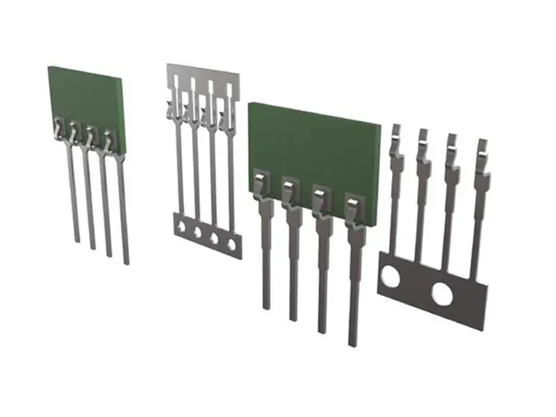
What Each Process Does to the Metal
Stamping cuts and forms lead frames with a die: a punch pushes the strip through a mating die cavity, shearing the metal. The cut edge is really two zones. In the burnished shear zone the punch does the work, compressing and cold-working the metal for roughly one-third of the thickness. Below it, the fracture zone tears as the punch breaks through, leaving a slightly rougher surface and a burr on the exit side. The balance between the zones depends on die clearance — typically 4 to 10 percent of stock thickness per side (typical) — and the burr must be oriented and controlled in the die design.
Etching dissolves metal chemically. A photoresist pattern is exposed and developed onto the strip, then etchant removes the unprotected metal from both sides simultaneously. Because the etch attacks laterally as well as vertically, the edge ends up rounded and slightly tapered — a characteristic cross-section that no shear burr can match. But there is also no work hardening, no burnished zone, and no residual compressive stress at the edge.
These are not cosmetic differences. In a power module, the lead frame edge sits inside the mold compound, carries bond wire terminations, and transfers heat to the DBC substrate. Whether that edge is shear-hardened or stress-free changes fatigue behavior, solder wetting, and coplanarity stability. The process decision is a material-science decision, not a sourcing preference.
| Feature | Progressive die stamping | Chemical etching |
|---|---|---|
| Material removal | Shear + fracture (mechanical) | Chemical dissolution (both sides) |
| Edge profile | Burnished shear zone + fracture + burr | Rounded, tapered, burr-free |
| Edge metallurgy | Work-hardened, residual compressive stress | Stress-free, no cold work |
| Typical stock thickness | 0.08 – 4.0 mm | 0.025 – 0.25 mm (typical) |
| Lead time to first article | 4 – 6 weeks (die build) | 1 – 2 weeks (artwork) |
| Throughput | Up to 800 SPM | Batch panels, minutes per panel |
The Capability Matrix
Put both processes on one table with the numbers that matter at a quote review: tolerance, feature density, material range, and the cost inputs that drive the decision. The stamping figures below are what a controlled progressive die line delivers under IATF 16949; the etching figures are typical published process capability.
| Parameter | Stamping (progressive die) | Chemical etching |
|---|---|---|
| Critical feature tolerance | ±0.005 mm (CMM verified, Cpk ≥ 1.67) | ±0.025 mm typical |
| Die pad coplanarity | < 0.05 mm maintained in-die | Flat, but warpage risk on thin strip |
| Burr height | < 15 µm (typical, controllable) | None — rounded edge by nature |
| Minimum feature width | ≈ 0.5 × stock thickness (typical) | ≈ 1 × stock thickness (typical) |
| Material thickness range | 0.08 – 4.0 mm | 0.025 – 0.25 mm typical |
| Materials | C1100, C194, C7025, Alloy 42, brass, steel | Same alloys, plus very soft tempers |
| Tooling cost | USD 20k – 200k+ (typical) | Near zero (artwork films) |
| Tooling life | 10M+ strokes with in-house maintenance | Artwork re-filmed per order |
| Per-piece cost at 1M/yr | USD 0.05 – 0.15 (typical) | USD 0.20 – 0.60 (typical) |
Read the matrix as a set of constraints, not a scorecard. Etching wins on thin stock and fine features; stamping wins on tolerance consistency, throughput, and mechanical edge properties. Most production lead frames end up stamped for the last three reasons.
Tolerance and Edge Quality, Deep Dive
The tolerance story is where programs get into trouble, because both processes can quote similar numbers while delivering different realities.
Stamping tolerance is a function of die precision and machine stability. A progressive die with precision-ground stations, guided strippers, and in-die coining holds critical features to ±0.005 mm for millions of strokes, with CMM sampling and SPC holding Cpk at 1.67 or higher. The tolerance is locked in steel; it drifts slowly with die wear, and it is corrected by scheduled maintenance rather than by process tuning. Burr height stays below 15 µm (typical) when clearance is maintained, and burr direction is controlled by the die.
Etching tolerance is a function of chemistry and artwork. The etchant removes material laterally while cutting through the thickness, so the as-etched feature is narrower than the artwork by the etch factor — typically 1.5 to 2.5 times the etch depth per side, depending on etchant, temperature, and agitation. The supplier compensates in the artwork, but the compensation is itself a process variable: if the etch rate drifts, the feature drifts. Real-world etching holds ±0.025 mm (typical) with good process control, and the edge taper is inherent.
For a power module die pad, the practical question is not the printed tolerance but the assembled flatness. A stamped frame holds coplanarity below 0.05 mm through in-die coining; an etched frame depends on strip temper and handling, because there is no die to force flatness. When the die-attach process is silver sintering — which demands a void-free interface — the coplanarity advantage of stamping shows up directly in module yield.
Material Behavior: How Alloys React
The same alloy behaves differently under the two processes, and the alloy choice can flip a borderline decision.
| Alloy | Typical use | Stamping behavior | Etching behavior |
|---|---|---|---|
| C1100 ETP copper | Power leads, high-current frames | Excellent; 101% IACS, clean shear, easy coining | Excellent; uniform etch, soft temper etches fast |
| C194 HSM copper | Lead frames, high-strength need | Excellent; spring temper holds flatness | Good; stronger etchant resistance, slower etch |
| C7025 (C70250) | Thin high-strength frames | Good; hard temper, tighter bend radius limits | Good; fine features achievable |
| Alloy 42 (NiFe) | Ceramic-compatible, power cycling | Fair; harder, higher die wear, burr control critical | Excellent; etch is the classic route for thin Alloy 42 |
| Brass / phosphor bronze | Signal and connector frames | Excellent; low cost, easy forming | Good; moderate etch rate |
Alloy 42 deserves special attention. Its low thermal expansion matches ceramic and silicon, which makes it the classic choice for power-cycling-sensitive modules. But it is harder and more abrasive than copper, so stamping it means higher die wear and stricter burr control. Below 0.10 mm thickness, etching is often the practical route for Alloy 42, and many suppliers quote it that way by default. Above 0.15 mm with real volume, stamping still wins on cost — with a tool-steel die specified for the abrasive NiFe.
Copper tempers matter too. Half-hard and spring-temper C194 strips stamp cleanly and hold flatness; fully soft strip tends to smear at the shear zone and needs tighter clearance control. On the etch side, soft tempers etch faster and more uniformly, which is why R&D frames in soft C1100 are cheap and fast to make — and why the same soft material can be hard to stamp at volume.
When Stamping Wins
Choose progressive die stamping when any of these conditions hold:
- Volume is real. Above roughly 50,000 pieces per year, the die amortizes and stamping unit cost drops to 3 to 10 times below etching (typical). At 500M+ parts per year capacity, a progressive line is the only economic answer.
- You need tight, repeatable geometry. ±0.005 mm on critical features with Cpk ≥ 1.67 is routine on a controlled line; an etch house quoting the same tolerance is quoting special capability at special price.
- Die pad flatness decides module yield. In-die coining and bottoming control coplanarity below 0.05 mm run after run, which protects the silver-sinter or solder die-attach interface.
- The edge must carry load. The work-hardened shear edge resists bending fatigue where bond wires terminate, and the burnished zone gives a consistent surface for selective plating.
- You want one supplier for strip, stamping, plating, and forming. A single factory with in-house tooling keeps die iterations measured in days and PPAP documentation under one roof.
EV power modules are the clearest case. At 800 V system voltage and hundreds of amperes, coplanarity, burr, and traceability are mission-critical, and volumes justify tooling. The industry norm for production power module lead frames is stamping — etching appears mainly in R&D, pre-production, or very thin specialty frames.
When Etching Wins
Choose chemical etching when any of these conditions hold:
- You are prototyping. First-article lead frames in 1 to 2 weeks from artwork, with the same alloy and roughly the same geometry as production, let you validate die attach and wire bonding before committing to a die.
- Volume is below the crossover. Below about 50,000 pieces a year, a USD 68,000 die adds more to the part than the etch premium saves. Run the math per part, not per feeling.
- Stock is very thin. Below 0.08 mm, stamping edge quality degrades and etching becomes the practical route (typical practice).
- Features are finer than stamping can hold. Dense finger arrays with feature widths below half the stock thickness are often etch-only.
- Burr is unacceptable in any orientation. Some fine-pitch applications cannot tolerate a burr at all, and etching eliminates the variable by nature.
The honest caveat: etching gives up the mechanical edge, the tolerance band, and the throughput. Use it where those three do not matter — and migrate to stamping when volume and yield tell you to. The cleanest pattern is an etch-to-stamp transition: etch the prototypes, validate the module, then cut the die and let tooling amortization do its work.
The Hidden Trade-offs
Three trade-offs hide beneath the obvious comparison, and each one has burned a program before.
1. The crossover is a band, not a line. The 50,000 to 100,000-piece crossover shifts with feature density and material. A complex, fine-feature frame favors etching longer; a simple thick-copper frame favors stamping earlier. Model both quotes at your actual annual volume and at a 2-year horizon before choosing.
2. Plating behaves differently on the two edges. Selective strip plating wets the burnished shear zone consistently, but the fracture zone can plate thicker or thinner depending on die condition. Etched edges plate evenly by nature, yet the rounded profile changes contact geometry. Specify plating thickness on the functional surface and verify with cross-section, not with a coat-weight average.
3. Etch taper is a tolerance thief. A 0.15 mm strip etched from both sides loses lateral material in the etch, so the as-etched finger is narrower than the artwork by roughly the etch factor. The supplier compensates in the artwork, but the compensation itself is a process variable. Stamping holds the width in steel and keeps it there for 10 million strokes.
| Scenario | Stamping unit cost (typical) | Etching unit cost (typical) | Winner |
|---|---|---|---|
| 10,000 pcs/yr, 0.10 mm Alloy 42 | USD 6.90+ (tooling amortized) | USD 0.80 – 1.50 | Etching |
| 150,000 pcs/yr, 0.20 mm C194 | USD 0.25 – 0.45 | USD 0.60 – 1.20 | Stamping |
| 1M+ pcs/yr, 0.25 mm C1100 | USD 0.05 – 0.15 | USD 0.20 – 0.60 | Stamping |
The Total Cost Model
A unit-price comparison hides the real economics. The decision that matters is total cost over the program life, and the formula is simple: total cost = tooling + (unit price × annual volume × program years) + yield-loss cost. Run it at two or three volume scenarios before choosing.
Take a 0.20 mm C194 frame quoted at USD 0.08 stamped versus USD 0.45 etched, with a USD 60,000 die and a 5-year program:
| Scenario | Stamping total (5 yr) | Etching total (5 yr) |
|---|---|---|
| 100,000 pcs/yr (500k total) | USD 60,000 + USD 40,000 = USD 100,000 | USD 225,000 |
| 500,000 pcs/yr (2.5M total) | USD 60,000 + USD 200,000 = USD 260,000 | USD 1,125,000 |
| 2M pcs/yr (10M total) | USD 60,000 + USD 800,000 = USD 860,000 | USD 4,500,000 |
The crossover is stark. At 100,000 pieces a year the die pays for itself inside the program; at 2 million a year the etched choice burns over USD 3.6 million extra over five years. Now add yield: a stamped frame at Cpk ≥ 1.67 ships fewer sort rejects than an etched frame chasing a tolerance it holds at ±0.025 mm typical, and every rejected lot carries sorting, reinspection, and line-down cost that rarely appears in the unit price.
One more input belongs in the model: the die can be reused. A progressive die for a frame family, with interchangeable stations, serves multiple part numbers and future revisions. The etch house re-films artwork every order, forever. Tooling is an asset; artwork is an expense.
The Six-Question Decision Checklist
When a frame program lands on your desk, work this list in order. It takes ten minutes and prevents the two failure modes at the top of this article.
- 1. What is the honest annual volume? Not the launch forecast — the 3-year contracted volume. Below ~50k, etching; above ~100k, stamping; in between, model both.
- 2. What thickness and temper? Below 0.08 mm, etching is usually the practical route. Above 0.15 mm with volume, stamping. Soft temper favors etching; spring temper favors stamping.
- 3. What does the die pad need? Coplanarity below 0.05 mm for sinter attach, or looser for solder? Tighter flatness points to stamping with in-die coining.
- 4. Is the edge a functional surface? Bond wire termination, solder fillet, or contact? If yes, decide whether you want work-hardened (stamping) or stress-free (etching) edge metallurgy.
- 5. Does the alloy fight the process? Alloy 42 below 0.10 mm, soft C1100, or very fine features favor etching; C194/C7025 at volume favor stamping.
- 6. Who owns the tooling and the traceability? A single factory that stamps, plates, and documents under IATF 16949 shortens the chain and the PPAP file. An etch subcontractor adds a hand-off.
Plating and Post-Processing
Whatever the forming process, the lead frame leaves the stamping or etching house for plating. The interaction between forming process and plating is part of the selection.
Selective strip plating applies silver, tin, nickel, or gold only where the module needs it — the die pad for sinter or solder attach, the lead tips for wire bonding, the outer leads for board assembly. Typical thicknesses run 1 to 8 µm for silver and tin, 0.1 to 1.5 µm for gold, and 1 to 10 µm for nickel. Selective plating cuts precious-metal usage by up to 90 percent versus full plating, which is why virtually every production power module frame uses it.
Stamping interacts with plating through edge condition. The burnished zone plates uniformly; the fracture zone can plate slightly differently, and a worn die with heavy burr will show it. The answer is not to avoid stamping but to control burr height below 15 µm (typical) and orient the burr away from functional surfaces — both die-design decisions. Etched edges plate evenly but have a larger surface area from the taper, so the same specified thickness uses slightly more metal.
Post-processing also includes deflashing after molding, lead trimming, and 100 percent coplanarity inspection. A stamped frame with consistent geometry simplifies all three; an etched frame with taper variability adds inspection time downstream.
Quality and Verification
The verification plan is the same for both processes, and the pass/fail behavior differs.
- Dimensional inspection: CMM and vision systems measure critical features and coplanarity. Stamping holds tighter Cpk with the same sampling plan; etching needs larger samples to catch etch-rate drift.
- Burr and edge inspection: Vision systems check burr height and direction on stamped frames. Etched frames skip burr checks but need edge-profile sampling to confirm taper is within compensation.
- Plating verification: X-ray fluorescence (XRF) measures coat thickness on functional surfaces; cross-sections confirm coverage on the edge zones. This is where plating defects — like the 2 µm versus 8 µm discrepancy that triggered a 40,000-vehicle recall — get caught before shipment.
- Traceability: IATF 16949 programs require lot traceability from strip coil to finished frame. A single-factory stamping line keeps the chain short; an etch subcontractor adds a hand-off in the middle.
- Reliability tests: Thermal cycling, power cycling, and high-temperature storage (typical: 1000 cycles at -40 to 150 °C) validate the frame in the module. The frame process is an input to module qualification, so the process decision must be locked before qualification starts.
The Final Call
Etch the prototype, stamp the production part. Match the process to the volume curve, and hold the supplier to the tolerance band in the matrix above — a stamping line under IATF 16949 delivers ±0.005 mm with Cpk ≥ 1.67, while etching stays honest at ±0.025 mm typical.
Send us your lead frame drawing for a stamping versus etching quote on the same part — with the volume crossover marked on it.
NEXT STEP
Ready to Manufacture Your Part?
Send us your drawing or sample — our engineers return DFM feedback within 24 hours with pricing and lead time from our IATF 16949 factory.
Written by
Ray Chan
Manufacturing engineer at KRAVZIK (Dongguan Guohong Precision). Writes shop-floor guides on progressive-die stamping, injection molding and precision component sourcing for global OEM buyers.