
Ultra-Precise Copper Plating Turnkey Solutions
Overcoming inherent electrochemical challenges such as uneven mass transfer on complex geometries and poor interfacial adhesion across diverse substrates, we engineer high-purity, ductile copper layers that ensure maximum electrical and thermal conductivity. By utilizing automated plating lines and…
Overcoming inherent electrochemical challenges such as uneven mass transfer on complex geometries and poor interfacial adhesion across diverse substrates, we engineer high-purity, ductile copper layers that ensure maximum electrical and thermal conductivity. By utilizing automated plating lines and maintaining precise chemical bath equilibrium, our workflows translate raw substrate conductive limitations into high-performance pathways optimized for critical electronic connectors. Backed by our rigorous IATF 16949-certified quality framework, we guarantee 100% molecular bonding integrity across all post-processing stages, thereby eliminating delamination risks and ensuring flawless execution under demanding signal transmission tolerances.
Superior Conductivity: High electrical and thermal transmission efficiency.Exceptional Adhesion: Robust bonding for specialized multi-layer plating.Uniform Deposition: Precise thickness control for complex part geometries.Enhanced Solderability: Optimized surfaces for reliable electronic assembly.Request DFM Evaluation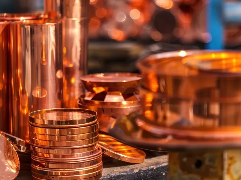
What is Copper Plating & The Science of High-Conductivity Surfaces
Copper plating is a sophisticated electrochemical process that deposits a layer of high-purity copper onto metallic or non-metallic substrates. Renowned for its exceptional electrical and thermal conductivity, copper serves as both a functional final finish and a critical "strike" underlayer for multi-stage plating. By utilizing precise electrolytic baths, this process ensures superior ductile properties and atomic-level bonding, making it the industry standard for high-performance electronic connectors, power distribution components, and intricate automotive stamping parts.
Precision Pre-Treatment & Activation
Raw components undergo a rigorous multi-stage cleaning process involving ultrasonic degreasing and electrolytic cleaning to eliminate residual lubricants from the stamping or molding phase. This is followed by specialized acid activation to remove surface oxides, creating a chemically active substrate essential for preventing delamination and ensuring a flawless, pore-free copper molecular bond.
Regulated Electro-Deposition
Components are submerged in a highly stable electrolytic copper bath (acidic or cyanide-free) where controlled DC current density drives copper ions to settle uniformly. Our automated lines utilize constant agitation and filtration to manage ion concentration, ensuring consistent coating thickness even within the deep recesses and complex geometries of custom-engineered terminals and heat sinks.
Anti-Tarnish & Surface Stabilization
Due to copper’s natural susceptibility to oxidation, every part is treated with a specialized organic anti-tarnish film or a passivation dip. This critical protective barrier seals the copper surface, preserving its high-luster appearance and maintaining its superior solderability and conductivity for extended storage and subsequent assembly processes.
Metrological & Integrity Validation
Every batch is verified through non-destructive X-ray Fluorescence (XRF) for exact thickness compliance. Beyond dimensional checks, we perform rigorous bake-and-quench or tape-pull adhesion tests to ensure the plating integrity meets IATF 16949 standards. Final inspection also confirms 100% RoHS/REACH compliance, guaranteeing a surface that is as safe as it is high-performing.
Advanced Copper Plating Specifications & Capabilities
Kravzik delivers high-purity copper deposition with atomic-level bonding precision. Our specialized electrolytic lines are engineered to meet the stringent electrical conductivity and thermal dissipation requirements of the EV battery, telecommunications, and medical device sectors, ensuring consistent performance across high-volume production runs.
Request DFM EvaluationCoating Thickness Range
2.5μm – 50μm+ (0.1 – 2.0 mil) tailored for strike layers or heavy-build functional applications.
Dimensional Tolerance Control
±0.0025mm (±0.1 mil) precision maintained for high-density electronic connectors and micro-stamping.
Substrate Versatility
Certified processes for Steel, Stainless Steel, Aluminum, Zinc Die-Cast, and specialized Plastics (ABS).
Adhesion & Integrity
Meets ASTM B571 standards; guaranteed zero peeling or blistering during high-heat soldering or cycling.
Surface Finish Options
Available in Bright (High-Luster), Semi-Bright (Satin), and Matte (Functional/Under-plate) finishes.
Maximum Processing Capacity
Equipped with both high-capacity Rack Plating for large components and Barrel Plating for mass-produced small parts.
Compliance & Testing
100% RoHS & REACH compliant; IATF 16949-certified quality control with in-house XRF thickness verification.
Electrical Conductivity
≥ 100% IACS purity levels, ensuring minimal contact resistance for power distribution components.
Advanced Substrate Compatibility & Metallurgical Integration
The performance of a copper coating—specifically its atomic-level adhesion and interface conductivity—is dictated by the electrochemical compatibility of the base metal. Kravzik engineers implement substrate-specific activation protocols to overcome inherent metallurgical barriers such as passive oxide layers in aluminum or surface porosity in die-castings, ensuring a robust molecular bond for every precision stamped or molded component.
Aluminum Alloys (6061, 7075, ADC12)
Standard aluminum naturally forms a persistent oxide layer that inhibits plating adhesion. Our specialized double-zincate immersion technique replaces this oxide with a thin zinc film, providing a stable foundation for subsequent copper deposition. This process is critical for heat sinks and lightweight EV battery busbars, ensuring zero delamination under high thermal loads.
Carbon & Alloy Steels (1018, 4140, 12L14)
High-strength steels are prone to rapid oxidation during the pre-plating phase, which can lead to poor electrical contact. We utilize a high-efficiency alkaline copper strike followed by a dense acid copper build-up. This two-stage approach provides a pore-free barrier and superior ductility, essential for heavy-duty industrial fasteners and precision-machined mechanical linkages.
Zinc Die-Castings (Zamak 3, Zamak 5)
Zinc die-cast parts often contain micro-porosity that can trap plating chemicals, leading to “out-gassing” and surface blistering. Our facility employs a specialized cyanide-free alkaline copper process that effectively “seals” the porous surface. This ensures a flawless, high-luster finish for decorative automotive trim and complex electronic housings without compromising structural integrity.
Stainless Steel Series (304, 316, 430)
The chromium-rich passive film on stainless steel makes direct copper plating nearly impossible. We implement a rigorous Woods Nickel Strike or specialized high-acid activation to strip the passive layer and establish a metallic bond. This is vital for medical instruments and food-processing hardware where high-purity copper is required as a functional underlayer or anti-microbial surface.
Copper & Brass Alloys (C36000, C11000)
While chemically similar, these alloys require precise micro-etching to remove surface tarnishes and residual drawing oils. Our regulated acid-activation baths ensure a virgin metallic surface, maximizing the thermal and electrical interface efficiency. This makes our process the industry choice for high-frequency RF connectors and high-amperage power distribution terminals.
Engineering Plastics (ABS, PC-ABS)
To plate non-conductive molded parts, we utilize a multi-stage chemical activation process involving chromic etching and palladium-tin catalysts. This creates a conductive electroless copper seed layer onto which heavy functional copper can be deposited. This capability is essential for EMI/RFI shielding in telecommunications and lightweight decorative components for the automotive sector.
Essential Design Guidelines & Engineering Limitations for Copper Plating
Proactive design optimization prevents manufacturing delays and ensures your components meet critical electrical and thermal specifications. Consider these geometric and dimensional factors before finalizing your CAD models for the electrolytic copper plating process to ensure peak performance and cost-efficiency.
Copper plating adds a definitive layer of material to your component’s surface, typically ranging from 5μm to 25μm per side. Because internal and external threads experience dimensional changes up to four times the plating thickness on their pitch diameter, Kravzik engineers recommend specifying pre-plate allowances or utilizing slightly oversized taps for fine-threaded connectors to guarantee smooth mechanical assembly.
Electrolytic copper deposition relies on line-of-sight electrical current. Deep blind holes, narrow channels, and complex inner diameters will naturally receive a thinner coating than exterior surfaces due to limited “throwing power” and the “Faraday cage” effect. For components requiring internal conductivity, we advise designing auxiliary drainage/access holes or consulting our team to optimize specialized anode placement.
Electrical current naturally concentrates at sharp corners and exterior edges, leading to disproportionately thick copper deposits known as “buildup” or the “dog-bone effect.” To ensure a uniform finish and avoid interference in high-precision stamped terminals, engineers should incorporate generous radii (minimum 0.3mm) where possible. This prevents brittle edge deposits and ensures consistent contact resistance.
Many RF and power components require copper only on functional contact zones. While we offer precision masking using high-temperature tapes or custom-molded plugs, complex masking patterns increase labor and cycle times. We recommend designing parts with clearly defined transition zones and accessible “shut-off” surfaces to ensure sharp masking lines and prevent chemical seepage.
The plating process involves submersion in active chemical baths. Porous substrates, such as certain zinc die-castings or low-density molded parts, can trap these fluids. This trapped chemistry may eventually seep out—known as “bleed out”—causing localized oxidation and ruining the finish. Designing out deep pockets and ensuring high-density base materials is essential for a high-luster, stable copper surface.
VISUAL EXCELLENCEData-Driven Showcase: Engineered Copper Finishes
The electrical efficiency, thermal dissipation, and bonding integrity of a copper-plated component are dictated by the specific electrolytic chemistry and post-plate stabilization utilized. Explore our standard copper profiles to identify the precise functional specifications and visual finish required for your specific engineering assembly.
FUNCTIONAL FINISHBright Copper Plating
High ConductivitySuperior SolderabilityLow Contact ResistanceMirror FinishUtilizing high-purity copper anodes and specialized organic brighteners, this process yields a dense, mirror-like finish with exceptional leveling properties. It is the industry standard for high-frequency signal transmission where minimizing the "skin effect" and maximizing surface conductivity are paramount for performance.
Electrolytic ChemistryAcid Sulfate / High-Brightener SystemElectrical Conductivity≥ 101% IACS (International Annealed Copper Standard)Plating Thickness5 – 25 μm (Tailored to spec)Primary Engineering BenefitMinimal contact resistance with excellent decorative appeal.Ideal For:RF connectors, EV battery terminal pins, and high-end audio hardware.HEAVY-DUTY ENGINEERINGMatte Functional Copper
High DuctilityStress-Free BuildThermal DissipationPore-Free BarrierA sulfate-based process engineered for maximum grain refinement and minimal internal stress. This finish provides superior ductility, allowing the plated layer to withstand significant mechanical deformation and thermal cycling without cracking or delamination. It is ideal for heavy-build applications requiring extreme reliability.
Electrolytic ChemistryLow-Stress Acid Sulfate SystemElectrical Conductivity100% IACSPlating Thickness25 – 75+ μm (Heavy build capability)Primary Engineering BenefiExceptional thermal management and mechanical flexibility.Primary BenefitSuperior ductility and reliable molecular bondingIdeal ForPower distribution busbars, PCB thermal vias, and heat sink assemblies.BONDING & INTERFACECyanide-Free Copper Strike
Atomic AdhesionSubstrate SealingBarrier LayerUniform CoverageEngineered as a critical molecular bridge for "difficult" substrates such as zinc die-cast, aluminum, or steel. This alkaline chemistry effectively seals the substrate surface, preventing base-metal migration and providing a chemically active foundation that ensures 100% bonding integrity for subsequent nickel or precious metal layers.
Electrolytic ChemistryAlkaline Cyanide-Free StrikeAdhesion StrengthExceeds ASTM B571 Tape/Bake testsPlating Thickness2 – 5 μm (Thin-film barrier)Primary Engineering BenefitPrevents blistering and ensures flawless multi-layer adhesion.Ideal ForZinc die-cast housings, aluminum heat spreaders, and multi-stage plating strikes. Request DFM EvaluationView Surface Treatment SolutionsSERVICES LIBRARYExplore Other Industrial Surface Treatment & Finishing Services Available
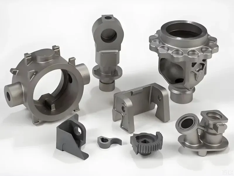
Nitriding
Forget brittle surfaces and dimensional warping. Kravzik delivers 1200 HV surface hardness while maintaining absolute ±5µm geometric precision.
Learn More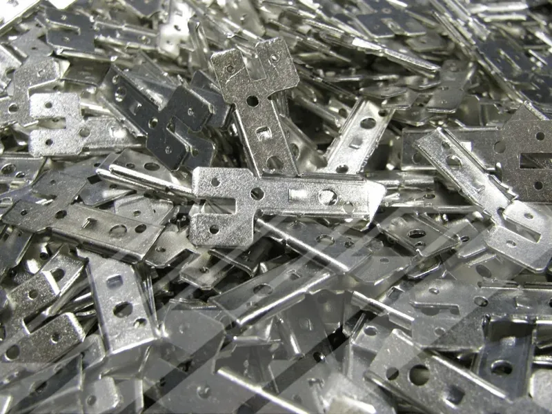
Tin Plating
Stop tin whisker failures in dense electronics. Our 150°C annealing process ensures 100% solderability for critical terminals.
Learn More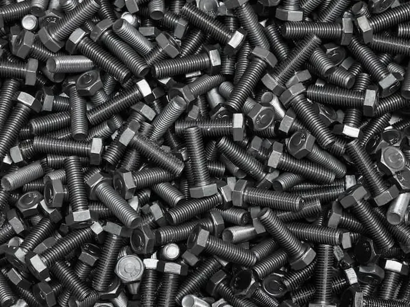
Black Oxide Coating
Stop reddish smut on precision tool steels. Our hot bath process ensures 0.000″ build-up for robotic vision systems.
Learn MoreRequest DFM EvaluationSee More Surface TreatmentTECHNICAL REFERENCEFrequently Asked Questions
Answers to common questions regarding precision, tooling, materials, and our integrated molding capabilities.We utilize a specialized double-zincate immersion technique to strip natural oxides and establish a stable metallic film, ensuring a robust molecular bond that prevents delamination during high-heat thermal cycling.
Our high-purity electrolytic copper plating consistently meets or exceeds 101% IACS standards, providing the ultra-low contact resistance required for mission-critical EV battery busbars and 5G telecommunications hardware.
Yes, our automated plating lines utilize advanced current density control to achieve a thickness precision of +/- 2.5 micrometers, ensuring perfect mechanical fit for high-density electronic connectors and micro-stamping components.
For high-carbon and alloy steel components exceeding 32 HRC, we implement immediate post-plating thermal baking protocols to effectively extract atomic hydrogen and eliminate the risk of delayed brittle fracture.
Every completed batch is treated with a specialized organic anti-tarnish film or passivation dip, creating a transparent protective barrier that preserves the high-luster surface and maintains excellent solderability for subsequent assembly.
We offer professional masking services using high-temperature tapes and custom-molded plugs, allowing us to confine copper deposition strictly to functional zones while maintaining sharp transition lines on complex stamped or molded parts.
Our facility is equipped with fully automated, high-capacity barrel lines for cost-effective mass production of small fasteners, alongside precision rack systems for larger, delicate components requiring individual handling and inspection.
Kravzik operates under a strict IATF 16949 quality management system, guaranteeing that all electrolytic copper processes and post-treatments are 100% RoHS and REACH compliant for global industrial distribution.

Still have questions?
Our engineering team loves solving complex problems. Chat with us or send your drawing for a review.
Request DFM EvaluationReady to Manufacture With One Accountable Factory?
From in-house tooling to high-volume production — stamping, molding, plating and assembly under one IATF 16949 roof. Send your spec and volume, get a quote within 24 hours.